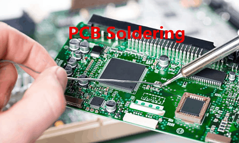
In today’s rapidly evolving electronics industry, printed circuit board (PCB) soldering is an essential process that requires meticulous attention to detail, especially for the successful functioning of electronic devices. With an increased demand for miniaturization, high performance, and reliable products, it’s crucial to focus on the issues and challenges involved in this integral part of electronics assembly.
This article delves into the top 10 issues we need to pay attention to in PCB soldering. By addressing these concerns, both professionals and hobbyists can take preemptive measures to achieve higher quality, consistency, and efficiency in their soldering endeavors, resulting in products that perform optimally and endure long-term use.
From solder materials selection to environmental considerations, we’ll explore the critical factors that must be understood and managed in order to improve soldering processes, ultimately leading to the production of superior electronic devices. As the technology landscape continues to develop, staying abreast of these key concerns will provide a solid foundation for success in the world of PCB soldering.
Understanding PCB Soldering
Soldering Basics
Printed Circuit Board (PCB) soldering is an essential process in electronics manufacturing. It involves joining electronic components together using solder, a metal alloy that typically consists of tin and lead, or lead-free alternatives such as tin-copper or tin-silver. Soldering plays a crucial role in creating a strong and reliable connection between components and the PCB.
The main types of soldering techniques are:
- Wave soldering: Used for through-hole component assembly
- Reflow soldering: Used for Surface Mount Technology (SMT) assembly
Both techniques require proper temperature control, solder paste composition, and consistent application to ensure optimal solder joints.
Soldering Techniques
There are several soldering techniques used in PCB assembly:
-
Manual soldering: Technicians use soldering irons and a hand solder wire to join components together. This method is suitable for small-scale production, repairs, and prototyping.
-
Wave soldering: PCBs with through-hole components are placed on a conveyor belt and passed through a wave of molten solder. The solder forms a bond between the component leads and the board’s copper pads.
-
Reflow soldering: A common technique for SMT assembly, reflow soldering involves applying solder paste to the PCB, placing the components on the paste, and then heating the assembly to melt the solder and create the connections.
Critical factors in successful soldering include:
| Factors | Importance |
|---|---|
| Temperature | Proper temperature ensures strong, reliable joints |
| Solder composition | Correct solder composition avoids defects and poor joints |
| Component alignment | Accurate placement improves reliability and performance |
By understanding the basics and techniques of soldering, we can work towards addressing the various issues that may arise in PCB soldering and improve the overall quality of electronic devices.
Soldering Materials

Soldering Alloys
Soldering alloys are crucial in creating strong and reliable connections between electronic components. They come in various compositions, each with their unique characteristics that affect durability, conductivity, and melting point. The most commonly used soldering alloys are:
- Tin-lead (Sn-Pb): Known for its low melting point and ease of use, tin-lead solder has been widely used in the electronics industry. However, due to increasing environmental concerns, lead-free soldering alloys are becoming more popular.
- Tin-silver-copper (Sn-Ag-Cu): This lead-free soldering alloy offers excellent melting and wetting properties, making it a suitable alternative to tin-lead solder.
It is essential to choose the right soldering alloy for your specific application to ensure proper solder joint formation and long-lasting connections.
Fluxes
Flux is a vital component in PCB soldering as it helps to remove surface impurities and enhance the flow of solder. This makes it easier for the solder to wet the metal surfaces, creating a strong bond between components. There are several types of fluxes used in PCB soldering, including:
- Rosin flux: Derived from natural pine resin, rosin flux is non-corrosive and has a long shelf life. It’s commonly used in electronics due to its reliable performance and low residue.
- Water-soluble flux: As the name implies, this flux can be cleaned off with water after soldering. This makes it an attractive option for PCB assembly, as no harmful chemicals are required for cleaning.
Understanding the properties of different flux types will allow you to choose the most suitable flux for your soldering needs.
Solder Paste
Solder paste plays a pivotal role in surface mount technology (SMT) by holding components in place before they are soldered. It comprises of tiny solder particles suspended in a sticky flux medium. When heated during the reflow process, the solder paste melts, forming reliable solder connections. Some key factors to consider when selecting a solder paste include:
- Composition: Select a solder paste with an alloy that matches your desired melting point and wetting properties.
- Viscosity: A suitable viscosity will ensure proper stencil printing and component placement without excessive spreading or slumping.
- Shelf life: Solder paste has a limited shelf life, so it’s essential to store it properly and use it before it expires to avoid defects and poor solder joints.
By paying close attention to these factors, you can ensure that your PCB soldering process is set up for success.
Solder Joint Quality
Evaluating Quality
To ensure a reliable PCB soldering process, it’s crucial to evaluate solder joint quality. Visual inspection is the most common method to assess the quality of a solder joint. In some cases, X-ray inspection or other non-destructive testing techniques may be used.
When evaluating quality, consider the following factors:
- Wetting: The solder should spread evenly and adhere well to the pads and components.
- Fillet Shape: Look for smooth and uniform fillets with no voids or cracks.
- Solder Volume: The solder joint should have sufficient volume to provide a strong mechanical and electrical connection.
Common Defects
Several common defects can occur in PCB soldering, negatively affecting the overall quality of the solder joint. Some of these defects include:
- Cold Solder Joints: These occur when the solder does not reflow properly, resulting in a weak connection. Causes may include insufficient heat, poor wetting, or excessive oxidation.
- Solder Bridges: This defect occurs when solder connects adjacent joints, creating an unintended electrical connection. It can result from excessive solder, improper reflow, or misaligned components.
- Voiding: Voids form when air or gas is trapped within the solder, weakening the joint. They can result from outgassing, flux entrapment, or poor wetting.
By paying close attention to solder joint quality and addressing these common defects, you can create strong, reliable connections in your PCB assembly process.
Thermal Management
Thermal Profiling
Thermal profiling is a critical aspect of PCB soldering as it helps establish the optimal temperature settings for various soldering processes. It is essential to monitor the temperature throughout various stages – such as the preheat, reflow, and cool down phases – to ensure consistent soldering quality.
- Preheat phase: a slow and steady temperature increase prepares the components and PCB for soldering
- Reflow phase: reaching the peak temperature needed to melt the solder paste, forming reliable solder joints
- Cool down phase: controlled cooling helps prevent thermal shock and ensures solidification of the solder joints
Having a well-planned thermal profile ensures proper wetting of solder, minimizes defects, and improves the overall quality of the solder joints.
PCB Material Considerations
The ability of the PCB material itself to dissipate heat is a critical factor in achieving successful soldering. FR-4 PCBs, for example, are often used due to their good thermal properties. Some considerations when choosing a PCB material include:
- Thermal conductivity: the material’s capacity to transfer heat within the PCB, influencing temperature gradients and soldering quality
- Coefficient of thermal expansion (CTE): the extent to which the material expands or contracts due to temperature variations, impacting dimensional stability during soldering
- Glass transition temperature (Tg): the point at which the material changes from being rigid to becoming increasingly flexible, affecting solder joint stability
Selecting the appropriate PCB material for your soldering process will ensure better thermal management, reducing the risk of soldering defects and increasing overall product reliability.
Component Placement
Orientation and Spacing
Proper orientation and spacing of components is crucial when soldering printed circuit boards (PCBs). Ensuring the correct orientation of components prevents any functional issues and enhances the performance of the board. It is essential to follow the manufacturer’s datasheets and guidelines for optimal orientation.
Spacing is equally important to avoid any unintended electrical or thermal connections between components. Adequate spacing can prevent short circuits and improve heat dissipation. A good rule of thumb is to maintain at least 1mm of clearance between components.
Surface Mount vs. Through-Hole
There are two primary methods of attaching components to PCBs: surface mount technology (SMT) and through-hole technology (THT).
SMT: This method involves soldering components directly onto the surface of a PCB. SMT is popular because it allows for small-sized components, high-density circuits, and faster assembly. However, it may require specialized equipment and skilled technicians.
- Key considerations:
- Accurate component placement: Use precise machinery or skilled manual labor to ensure accurate SMT soldering.
- Solder paste application: Proper stencil design is essential to achieve the right amount of solder paste on each pad.
- Key considerations:
THT: Components in through-hole technology have leads that are inserted into drilled holes on the PCB and soldered on the opposite side. THT is more robust and resistant to mechanical stress, making it suitable for applications requiring higher reliability or more substantial components.
- Key considerations:
- Hole size: Ensure the correct hole size for the component leads to ensure a secure, robust connection.
- Soldering technique: Use proper soldering methods (wave soldering or selective soldering) to create high-quality joints that can withstand stress.
- Key considerations:
Reducing Contamination
Contamination during PCB soldering is a crucial issue that can cause defects and lower the quality of the final product. To tackle this problem, it is essential to focus on proper storage practices and effective cleaning techniques.
Proper Storage
Adequate storage conditions are key to minimizing contamination in PCB soldering. Follow these guidelines for optimal results:
- Store PCBs in clean, cool, and dry environments.
- Use anti-static bags to protect boards from electrostatic discharge (ESD).
- Sealed containers are recommended to prevent dust and debris accumulation.
- Handle boards with clean hands or gloves to avoid transferring contaminants.
Cleaning Techniques
Implementing effective cleaning methods can further reduce contamination and ensure the longevity of PCBs. Some recommended practices include:
- Using ultrasonic baths with appropriate cleaning agents to remove contaminants.
- Applying air knives or compressed air to remove dust and loose particles.
- Utilizing a brush or lint-free cloth with isopropyl alcohol (IPA) for manual cleaning.
- Ensuring soldering equipment, such as soldering irons and tips, are cleaned regularly.
In summary, taking proactive steps to reduce contamination through proper storage and cleaning techniques can significantly improve the quality and performance of PCBs. By following these guidelines, you can avoid defects and ensure the long-term integrity of your soldering work.
Environmental Factors
Temperature and Humidity
In the PCB soldering process, temperature and humidity are crucial factors that can impact the soldering quality. Variations in temperature can cause thermal expansion and contraction of the materials, potentially leading to cracks in the solder joints.
- Ideal temperature range: 20-25°C (68-77°F)
- Ideal humidity range: 40-60% relative humidity
To maintain these optimal conditions, it is essential to implement temperature and humidity control systems in the soldering area.
Electrostatic Discharge
Electrostatic discharge (ESD) is another environmental issue that needs attention during PCB soldering. Static charge can accumulate on materials and tools, which may result in electronic components getting damaged.
To minimize the risk of ESD, several preventive measures can be implemented:
- Ensure grounding of equipment and soldering station
- Use ESD-safe tools, mats, and work surfaces
- Wear ESD-safe clothing and wrist straps
By addressing environmental factors such as temperature and humidity control and ESD prevention, the overall success of the PCB soldering process can be improved.
Fixture Design
Importance of Fixtures
Fixtures play a crucial role in the PCB soldering process. They ensure proper alignment of components and maintain stability during soldering. A well-designed fixture helps in achieving consistent solder joints, reducing defects, and improving overall productivity.
Fixture Selection
When choosing a fixture for PCB soldering, consider the following factors:
- Compatibility: Ensure that the fixture is compatible with the soldering equipment and process. Check for material specifications, dimensions, and other features.
- Ease of use: A user-friendly fixture minimizes the risk of errors and reduces the time required for setup and adjustments.
- Durability: Material used in the fixture should be able to withstand high temperatures and exposure to soldering chemicals without deforming or wearing out.
To summarize, a good fixture design is essential for successful PCB soldering. It helps ensure proper alignment and stability of components, leading to consistent solder joints and better productivity. When selecting a fixture, prioritize compatibility, ease of use, and durability.
Quality Control and Inspection
Quality control and inspection are crucial aspects of the PCB soldering process to identify potential defects and ensure a high level of performance for the final product. Various methods are implemented for efficient inspection and to detect anomalies.
Visual Inspection
Visual inspection is the initial step in quality control of PCBs. It involves technically trained professionals examining the solder joints, component placement, and connections to detect any potential issues at an early stage. Visual inspection factors include:
- Solder joint quality
- Correct component orientation
- Proper alignment of the components
Automatic Optical Inspection (AOI)
Automatic Optical Inspection (AOI) is a more advanced technique employed to inspect PCBs after the soldering process. It uses high-resolution cameras to take images of the board, which are then compared with a reference image to identify any discrepancies. AOI primarily detects:
- Missing or incorrectly placed components
- Incorrect solder paste application
- Bridges and insufficient solder
X-ray Inspection
X-ray inspection is employed to examine the finer details of PCB solder joints, especially in the case of BGAs and other hidden joints. It uses X-rays to effectively identify voids, cracks, and other defects that might not be visible through conventional visual inspection or AOI systems. X-ray inspection is essential for:
- Identifying voids and cracks in solder joints
- Examining hidden joints (e.g., BGAs)
- Evaluating the solder fillets
By implementing these inspection methods, quality control in PCB soldering can be ensured, leading to a higher level of performance for the final product.
Conclusion
PCB soldering is a crucial process in electronics manufacturing, and attention to detail is paramount for ensuring high-quality results. By acknowledging and addressing the following ten issues, professionals can produce more reliable and long-lasting electronic products.
Faulty connections, cold solder joints, and overheating are common problems that can be mitigated by adhering to proper temperature controls and soldering techniques. Selecting the right solder, flux, and tip size for the job can also improve the work quality and prevent potential issues.
The cleaning and maintenance of PCBs, soldering equipment, and workspace play a significant role in ensuring optimal soldering conditions. Using protective wear to avoid contamination is an essential measure.
Keeping these considerations in mind and diligently applying precise soldering practices can greatly enhance the outcome of a PCB soldering job, ultimately contributing to the production of better, more reliable electronic products.
