BGA (Ball Grid Array) is a type of PCB (Printed Circuit Board) layout that has become increasingly popular in recent years due to its numerous advantages. BGA is a type of surface-mount technology that uses small balls of solder to connect components to the board. This allows for a higher density of components, as well as improved electrical performance and thermal management.
One of the key benefits of BGA PCB layout is its ability to handle high-speed signals. Due to the shorter distance between components and the reduced inductance and capacitance, BGA can handle high-speed signals with less noise and better signal integrity. Additionally, BGA allows for a smaller board size, which can be especially important in applications where space is limited. This makes BGA an ideal choice for a wide range of applications, including consumer electronics, telecommunications, and medical devices.
What is BGA PCB Layout?
A Ball Grid Array (BGA) is a type of surface-mount packaging used for integrated circuits (ICs). In a BGA package, the IC is mounted on the printed circuit board (PCB) with solder balls that are arranged in a grid pattern on the bottom of the package. The solder balls are used to make electrical connections between the IC and the PCB.
The BGA PCB layout is the process of designing the PCB to accommodate the BGA package. This involves designing the PCB to have the correct number and placement of solder pads for the BGA package. The solder pads must be arranged in the same pattern as the solder balls on the BGA package.
BGA packages offer several advantages over other types of IC packages. They have a higher pin density, which means that more pins can be placed in a smaller area. This makes BGA packages ideal for high-performance applications where space is limited. BGA packages also have a lower profile than other packages, which makes them suitable for applications where height is a concern.
In summary, BGA PCB layout is the process of designing a PCB to accommodate a BGA package. BGA packages offer several advantages over other types of IC packages, including a higher pin density and a lower profile.
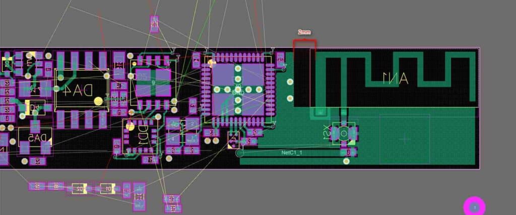
Design Considerations for BGA PCB Layout

When designing a printed circuit board (PCB) with a ball grid array (BGA) package, there are several design considerations that need to be taken into account to ensure a successful layout. These considerations include pad layout, via placement, and thermal considerations.
Pad Layout
The pad layout is critical for BGA PCB layout. The pad size, shape, and spacing must be optimized to ensure proper soldering and electrical connections. The pad size should be slightly larger than the ball size to allow for proper solder wetting. The spacing between the pads should be carefully calculated to avoid short circuits between adjacent pads.
Via Placement
Vias are used to connect the BGA pads to the other layers of the PCB. The via placement is critical for BGA PCB layout. The via size and spacing must be optimized to ensure proper electrical connections and to avoid thermal issues. Vias should be placed as close to the BGA pads as possible to reduce the inductance and resistance of the connection.
Thermal Considerations
Thermal considerations are critical for BGA PCB layout. The BGA package generates a significant amount of heat, and this heat must be dissipated to ensure proper operation. The PCB layout must be designed to provide a path for heat to flow away from the BGA package. This can be achieved through the use of thermal vias, copper pours, and heat sinks.
In conclusion, when designing a BGA PCB layout, it is important to consider the pad layout, via placement, and thermal considerations to ensure a successful design. By following these guidelines, you can create a reliable and efficient PCB layout that meets the requirements of your application.
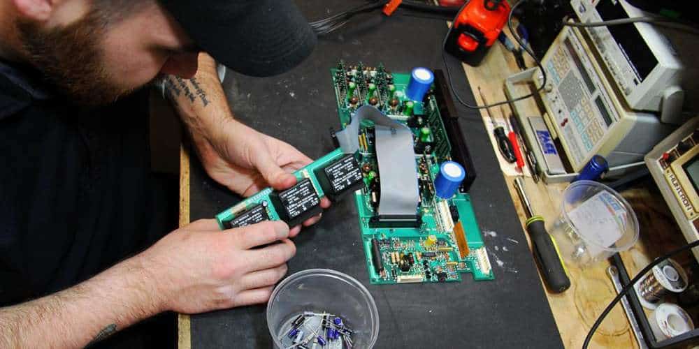
BGA Assembly Process
Solder Paste Application
The first step in BGA assembly process is the application of solder paste. The solder paste is applied to the BGA pads using a stencil. The stencil is placed over the PCB, and the solder paste is spread over the stencil using a squeegee. The solder paste is then removed, leaving a thin layer of paste on the pads.
Component Placement
The next step is the placement of the BGA components onto the PCB. The BGA components are picked up by a pick-and-place machine and placed onto the PCB. The machine uses a vision system to align the BGA components with the pads on the PCB. Once the BGA components are in place, the PCB is inspected to ensure that the components are correctly aligned.
Reflow Soldering
The final step in the BGA assembly process is the reflow soldering. The PCB with the BGA components is placed in a reflow oven, where the solder paste is melted and the BGA components are soldered to the PCB. The temperature and time of the reflow process are carefully controlled to ensure that the solder paste melts and solidifies properly.
During the reflow process, the BGA components are subject to thermal stress, which can cause them to warp or crack. To prevent this, the PCB is heated and cooled gradually, and the temperature is kept within a narrow range. After the reflow process, the PCB is inspected again to ensure that the BGA components are properly soldered to the PCB.
In conclusion, the BGA assembly process involves three main steps: solder paste application, component placement, and reflow soldering. Each of these steps is critical to the success of the BGA assembly process, and must be carefully controlled to ensure that the BGA components are properly soldered to the PCB.
BGA Inspection and Testing
BGA (Ball Grid Array) packages have become increasingly popular in PCB design due to their high pin count, small size, and low profile. However, BGA packages present unique challenges when it comes to inspection and testing. In this section, we will discuss the different methods used for BGA inspection and testing.
X-Ray Inspection
X-ray inspection is a common method used to inspect BGA packages. X-rays can penetrate the package and provide a detailed view of the solder joints and internal structure. This method is used to inspect the quality of the solder joints, verify the presence of solder balls, and check for voids or other defects. X-ray inspection is a non-destructive method and can be used to inspect the package both before and after assembly.
Optical Inspection
Optical inspection is another common method used to inspect BGA packages. This method involves using a microscope or camera to inspect the package for defects. Optical inspection can be used to verify the presence of solder balls, inspect the quality of the solder joints, and check for any visible defects. This method is typically used to inspect the package after assembly.
Functional Testing
Functional testing is a method used to test the performance of the BGA package. This method involves applying power to the package and checking the output signals. Functional testing can be used to verify the functionality of the package and check for any defects that may not be visible through X-ray or optical inspection.
In conclusion, BGA inspection and testing is crucial to ensure the quality and reliability of the package. X-ray inspection, optical inspection, and functional testing are the most common methods used to inspect and test BGA packages. Each method has its own advantages and disadvantages, and the choice of method depends on the specific requirements of the project.
Conclusion
In conclusion, designing a BGA PCB layout requires careful consideration and attention to detail. It is essential to follow the manufacturer’s guidelines and recommendations to ensure proper functionality and reliability.
One crucial aspect of BGA PCB layout design is the placement of vias. Vias should be placed away from the pads to avoid any interference with the soldering process. It is also essential to ensure that the vias are not placed too close to each other to prevent any short circuits.
Another critical factor to consider is the routing of the traces. It is recommended to use shorter traces and keep them as straight as possible to reduce signal delay and improve signal integrity. It is also essential to maintain a consistent trace width to prevent impedance mismatch and signal reflections.
Furthermore, it is crucial to pay attention to the thermal management of the BGA package. Adequate thermal relief and thermal vias should be used to ensure proper heat dissipation and prevent any thermal stress on the board.
In summary, designing a BGA PCB layout requires careful planning and attention to detail. By following the manufacturer’s guidelines and recommendations, considering the placement of vias, routing of traces, and thermal management, a reliable and functional BGA PCB layout can be achieved.
