Table of Contents
ToggleCircuit board fabrication is a complex process that involves designing, manufacturing, and assembling electronic circuits. The process begins with the design of the circuit, which is created using computer-aided design (CAD) software. The design is then printed onto a copper-clad board using a specialized printer that transfers the design onto the board.
Once the design is printed onto the board, the next step is to etch away the copper that is not part of the circuit. This is done using a chemical solution that removes the unwanted copper, leaving behind only the circuit. The board is then drilled to create holes for the electronic components, and a thin layer of solder is applied to the surface of the board to make it easier to attach the components.
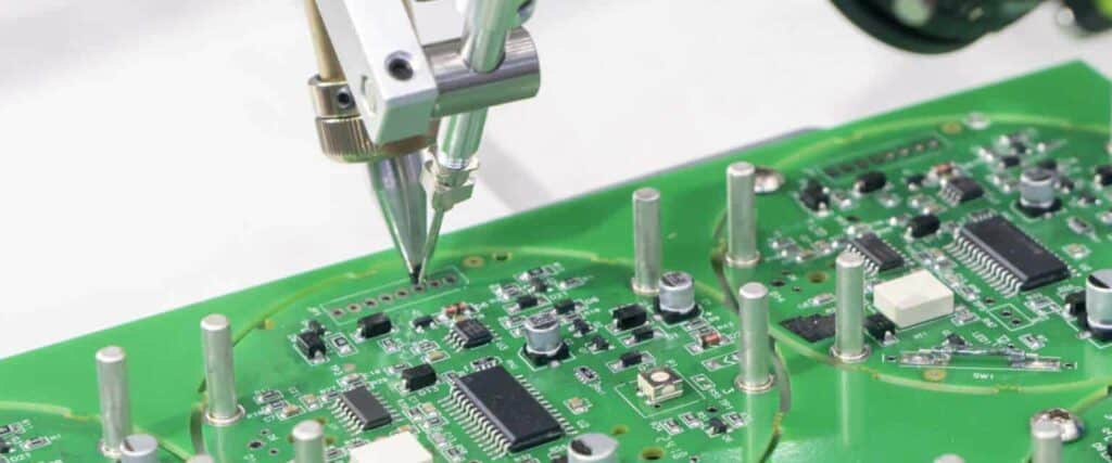
The final step in the circuit board fabrication process is to assemble the electronic components onto the board. This is done using a specialized machine that places the components onto the board and solders them in place. Once the components are attached, the circuit board is tested to ensure that it is functioning properly.

Basics of Circuit Board Fabrication
Materials Needed
Before starting the circuit board fabrication process, there are a few materials that you will need. These include:
- Copper-clad board
- Etching solution
- Transfer paper
- Toner-based printer
- Safety equipment (gloves, goggles, etc.)
- Drill and drill bits
- Soldering iron and solder
Designing the Circuit Board
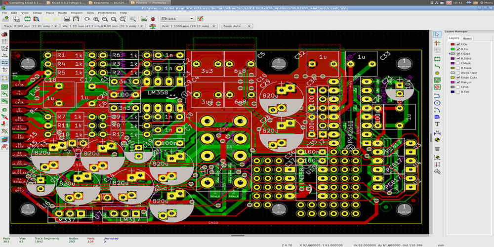
The first step in circuit board fabrication is designing the circuit board itself. This involves creating a schematic of the circuit and then laying out the board in a PCB design software.
Once the design is complete, the next step is to print out the design onto transfer paper using a toner-based printer. The transfer paper is then placed onto the copper-clad board and heated using a laminator or iron. This transfers the toner from the paper onto the board.
After transferring the design, the board is then etched using an etching solution. The etching solution removes the copper from the board that is not covered by the toner, leaving behind the circuit traces.
Finally, the board is drilled and the components are soldered onto the board. It is important to wear safety equipment during this process to avoid injury.
In conclusion, circuit board fabrication is a complex process that requires careful planning and attention to detail. By following the steps outlined above and using the necessary materials, you can create high-quality circuit boards for your electronic projects.
Circuit Board Manufacturing Process
Creating the Copper Layers
The first step in circuit board fabrication is to create the copper layers. This is done by laminating a thin layer of copper onto a substrate material, typically fiberglass or a composite material. The copper layer is then covered with a layer of photoresist, which is a light-sensitive material that will be used to create the circuit pattern.
Etching the Board
After the photoresist has been applied, the board is exposed to light through a mask that has the circuit pattern on it. The areas of the photoresist that are exposed to light harden, while the areas that are covered by the mask remain soft. The board is then washed with a chemical solution that removes the soft photoresist, leaving behind the hardened photoresist that protects the copper layer.
The board is then dipped in an etching solution that removes the unprotected copper, leaving behind the circuit pattern. The etching solution is typically an acidic solution that dissolves the copper, but there are also other etching solutions that can be used.
Drilling the Holes
Once the circuit pattern has been created, the board is drilled with small holes where components will be mounted. These holes are typically drilled with a computer-controlled drill that can drill holes with a high degree of accuracy. The holes are then plated with a thin layer of copper to create electrical connections between the different layers of the board.
Solder Mask Application
After the holes have been drilled, a solder mask is applied to the board. The solder mask is a layer of material that covers the copper traces and helps prevent solder from flowing where it shouldn’t during the assembly process. The solder mask is typically applied using a silk-screening process, which allows for precise application of the mask material.
Silkscreening
Finally, the board is silkscreened with any necessary markings or labels. This is done using a silk-screening process similar to the process used to apply the solder mask. The silkscreened markings can include component designators, company logos, and other information that helps identify the board.
Overall, the circuit board manufacturing process is a complex and precise process that requires a high degree of skill and expertise. By following these steps, circuit board manufacturers can create high-quality boards that meet the needs of their customers.
Quality Control and Testing

Visual Inspection
During circuit board fabrication, a visual inspection is performed to check for any defects in the board. This inspection ensures that the board is free from any scratches, cracks, or other damages that may affect its functionality. The inspection is carried out by trained personnel who use specialized equipment to detect any defects that may be present.
The visual inspection process involves checking the board’s surface for any imperfections that may affect its performance. The personnel performing the inspection look for any abnormalities, such as scratches, dents, or discoloration. Any defects found during the visual inspection are recorded and addressed before the board is sent for electrical testing.
Electrical Testing
After the visual inspection, the circuit board undergoes electrical testing. This testing is done to ensure that the board meets the required specifications and functions as intended. The electrical testing process involves applying voltage to the board and measuring the current flow and resistance.
The electrical testing process is carried out using specialized equipment, such as a multimeter or an oscilloscope. The equipment measures the voltage, current, and resistance of the board and compares them to the required specifications. If the board fails the electrical testing, it is sent back for repair or replaced.
In conclusion, quality control and testing are critical processes in circuit board fabrication. Visual inspection and electrical testing ensure that the board is free from defects and meets the required specifications. These processes ensure that the circuit board functions as intended and meets the customer’s needs.
Advanced Techniques

Multilayer Circuit Board Fabrication
Multilayer circuit boards are a type of PCB with more than two conductive layers separated by insulating material. They are used in high-performance electronic devices that require complex circuitry. Multilayer circuit board fabrication is a complex process that involves several steps.
The process begins with the design of the circuit board. The design is then transferred to a computer-aided manufacturing (CAM) system, which generates the necessary tool paths and data for the fabrication process. The layers of the board are then laminated together using heat and pressure. The next step is drilling, where holes are drilled through the board where components will be mounted. The board is then plated with copper to create the conductive pathways. Finally, the board is coated with a protective layer to prevent oxidation and damage.
Surface Mount Technology
Surface mount technology (SMT) is a method of mounting electronic components on a PCB. SMT components are smaller, lighter, and more reliable than traditional through-hole components. SMT components are mounted directly onto the surface of the PCB, rather than being inserted through holes in the board.
SMT components are mounted using a pick-and-place machine, which places the components onto the board with high precision. The components are then soldered onto the board using a reflow oven. SMT components can be placed on both sides of the board, which allows for more compact designs.
SMT technology has several advantages over traditional through-hole technology. SMT components are smaller, which allows for more compact designs. They are also more reliable, as they are less likely to come loose or break during use. SMT technology also allows for faster assembly times and lower costs.
In conclusion, multilayer circuit board fabrication and surface mount technology are advanced techniques used in the production of high-performance electronic devices. These techniques require specialized knowledge and equipment, but they offer several advantages over traditional methods.

