Ever wondered what the true essence of plating any object (especially electrical components) is? Components like wires, for example, are coated with resistors to guide the wire from corrosion and its handlers from shock. In this article, we will be discussing the essence and manufacturing process of plating copper on PCBs. Firstly let’s discuss what a PCB is.
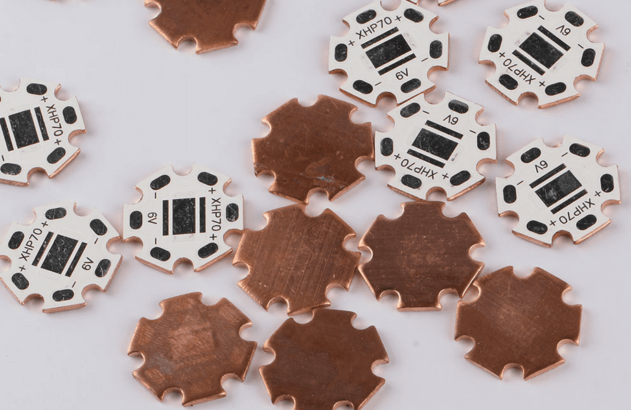
Overview of a Copper plate PCB
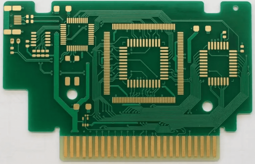
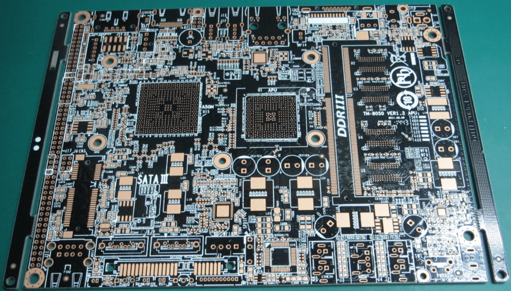
A printed circuit board (PCB) is an electronic system that utilizes copper circuits and sodium hydrogen sulfite solution to connect components electrically. Printed circuit boards (PCBs) support electronic components mechanically, allowing a device to be assembled in a frame. A printed circuit board structure must follow specific steps corresponding to the production process, integrated circuit assembling, and bare circuit board structure.
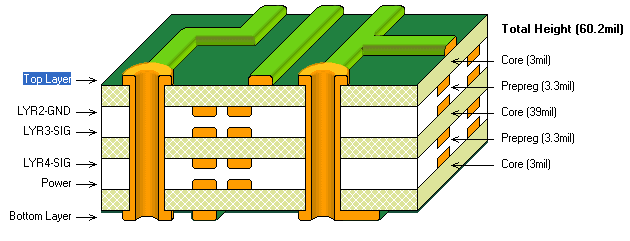
A Alu PCB comprises multiple layers of non-conductive and conductive materials that provide electrical interconnection throughout the circuit. Usually, hole walls are provided, and manufacturers sometimes prefer micro-etching with tin palladium colloid for surface energy.
One of these materials is the electroless copper plating that provides a resin surface for any other secondary activation process that may need to be done along the hole walls.
The conductive material, typically made of copper foil, is etched out of the inner layer pairs, producing only the circuitry patterns. After completing the process, these inner layers are laminated to form one composited board. The board is now drilled to develop holes for vias (vias are electrical interconnections between copper layers on Printed Circuit Boards (PCBs).
Vias are tiny drilled holes that connect several adjacent layers; the hole is usually plated with copper, which forms electrical connectivity through the insulation between the copper layers), and components. Once this is completed, the printed circuit board will be ready for plating copper in its through-holes and external layers.
What is Plating?
The electrochemical process of depositing a metal onto the printed circuit board’s surface and inside the plated through-holes is called electroless plating on Printed Circuit Boards (PCBs). Copper is the most commonly used plated metal in PCB fabrication which can be done with hexavalent chromium or palladium chloride.
Plating copper serves two functions; It increases the copper thickness of the exterior pads and conductors while also providing a strong copper connection between layers via the plated through-holes. The PCB design plays an important role in the type of plating and solder mask used.

Therefore, you can choose a square foot, contact area, surface area, or ground plane for your design. What matters is that the specific thickness should be used, and the correction liquor should be greatly increased.
Advantages of Copper Plating PCB
Before you consider copper plating PCB, you must be aware of the benefits you stand to enjoy from your decision based on the design rules available. Some notable advantages of copper plating by every possible design rule standard includes:
- Copper plating improves a PCB’s performance.
- It improves the sturdiness of via structures.
- It extends the life of the PCB by preventing structure failure.
- It improves via connectivity.
- It is a suitable plating material for all types of PCBs.
Copper Plating Processes
Many contract manufacturers have tested and trusted processes for designing circuit boards. However, the copper plating process is one that many of these manufacturers agree on because of how delicate it is.
The first PCB plating procedure will involve an electroless copper plating process that will chemically absorb the PCBs surface areas, including the interior of the bored holes. The primary objective of this plating copper process is to produce a thin copper foil framework and solder mask on the PCB and in the holes to function as the base for the electroplating process.
The board is now ready for electroplating, also known as Plated Through Hole (PTH), an autocatalytic redox reaction. The bored hole becomes the walls of a non-conducting substrate, onto which copper is chemically deposited for corresponding copper electroplating.
Procedures Involved in Preparing a PCB for Electroplating
- The holes are cleaned of drilling residues and contaminants.
- The holes’ interior is micro-etched to aid in chemical copper binding.
- A photoresist substance is then applied to the PCBs’ top and bottom.
- The photo-resistant surface is exposed to UV light, except for the circuit’s metallic to be plated.
- The spongy photoresist surrounding the circuit board is washed away, leaving the hardened photoresist to mask the remaining board surface areas.
Processes Involved in Electroplating in Simple Steps:
Step 1: Degreasing with Alkaline
- Charge Adjustment
- Washing
Step 2: is micro-etching
Step 3: Pre-impregnation
Step 4: Activation
Step 5: Peptization
Step 6: Electroless Plating of Copper
In Detail: The processed PCB is then connected to the electrical current’s cathode, or negative electrode, and submerged in a chemical bath for plating.
Dissolved chemical copper is now drawn through the liquid solution to the negative electrode and deposited into the bare copper circuitry on the PCB.
To ensure that the chemical copper is evenly applied, the board is dipped alternately into the plating and cleaning baths under controlled environments. After completing the copper plating, tin is coated on the copper layer to shield the circuit board. At the same time, the available photoresist will be stripped away, and the non-circuitry copper will be removed. Finally, the tin layer is removed, exposing the bare copper layer circuitry.
While this completes the copper plating process on the PCB, another crucial plating process is required to finish the production of the PCB.
Surface Finishing Processes for PCB Plating
To shield the bare copper, a surface finish is plated or applied over it. Different types of surface finishes can be applied on a PCB depending on the degree of protection required:
1. HASL (Hot Air Solder Leveling)
Application Process:
The PCB is dipped into a molten solder bath and rapidly passes through hot blasts of air to carefully extract excess solder.
Advantages of HASL
- It is a cost-effective operation
- It is available anywhere.
- Its process is easy and has a long shelf life.
Disadvantage of HASL
- The excess solder extraction process must deliver a detailed pitch component, which can cause solder bridging.
2. ENIG (Electroless Nickel Immersion Gold)
Application Process:
The process involves two layers of metal coatings; the first layer is chemically plated nickel. The nickel serves as a buffer for the copper foil, which is then shielded from oxidation by the second layer made of a thin layer of gold.
Advantages of ENIG
- It has clear planarity that makes it excellent for soldering its components
- It conforms to the RoHS requirements.
- It is long-lasting and durable.
Disadvantage of ENIG
- It is less economical than other finishes, such as HASL.
3. Immersion Silver
Application Process:
This surface finish is commonly used in high-speed PCBs because the silver has low failures in high-frequency components. Immersion silver is added to the copper layer through chemical analysis.
Advantages of Immersion Silver
- It also conforms to the RoHS requirements.
- It has an excellent surface finish ideal for clear-pitch soldering of components.
Disadvantages of Immersion Silver
- The finish process is sensitive to atmospheric contaminants and must be in air-tight packaging to reduce damage risk.
- Even with air-tight packaging, its shelf life is approximately 12 months, and it must be used immediately after removing its packaging.
Other Types of Surface Finishes In the PCB Plating Process Include:
- Lead-free HAS
- Organic solderability preservative (OSP)
- Immersion tin
- Hard gold
- ENEPIG – an abbreviation of Electroless nickel electroless palladium immersion gold
While each listed surface finish has specific uses, ENIG, HASL, and immersion silver are PCBs’ preferred surface finishes.
Important Factors To Consider During Copper Plating Pcb Manufacturing
1. Via height – influenced by PCB thickness
2. Fill type – influenced by via usage
3. Throwing power – ability to spread uniformly
4. Via diameter – influenced by surface-mounted device spacing and pitch
5. Plate thickness – affects durability and strength
6. Aspect ratio – the ratio of the board thickness and the via diameter
Applications of Heavy Copper PCBs
Copper PCB demand is driven by performance, ever-increasing power, and cost requirements. As a result, heavy copper-plated PCB is in high demand in computer, military, and industrial controls. Among the other applications are:
- Safety and signal systems
- Torque controls
- Solar power converters
- Renewable energies and storage pumping plants
- High power rectifiers
- Overload relays
- Traction converters for rail applications
- Power converters for railway systems
- Power line monitors
- UPS systems
- Protection relays
- Electric vehicle charging (commercial and industrial)
- Excitation systems for power regulators
- Position control systems
- Power grid switching systems
- Energy storage and power grid backup
- HVAC systems
- Nuclear power applications
- Line reactors
- Hydro-electric plants
- Weapons control systems
- Fuse blocks
- Surge protectors
- Welding Equipment
- Radar systems
Conclusion
Copper plating on a PCB requires extreme precision; considering all the PCB’s variables and specifications to determine the appropriate copper weight, copper thickness, and plating types is critical. Data required includes:
- Current estimations.
- Copper distribution.
- The size of the board.
- The type of PCB technology used.
Regarding surface planarity, considerations must be made for factors like the number of boards to be produced, the expected shelf life, and its expected application. The bottom line is that you need the best hands to handle the copper plating process to ensure no mistake is made. Talking about the best hands for your copper plating, contact Hillman Curtis today.
