KiCad is a popular open-source software suite that is widely used for designing printed circuit boards (PCBs). The software is free to use and offers a wide range of features that allow users to design complex PCBs with ease. One of the key features of KiCad is its ability to design 4 layer boards, which are becoming increasingly popular in the electronics industry.
A 4 layer board is a type of PCB that has four layers of copper traces and planes, sandwiched between layers of insulating material. These boards are used in applications where high-speed signals are required, as they offer better signal integrity and reduced electromagnetic interference (EMI) compared to 2 layer boards. With KiCad, users can easily design 4 layer boards by creating a stackup that specifies the thickness and material of each layer, and then adding the necessary components and traces.

Why Use a 4 Layer Board?
When designing a complex printed circuit board (PCB), you may need to use multiple layers to accommodate the necessary components and connections. A 4 layer board is an excellent choice for designs that require a high level of complexity and functionality.
Here are some reasons why you might want to use a 4 layer board:
-
Increased functionality: With four layers, you have more space to add components and connections, allowing you to create more complex designs with greater functionality.
-
Reduced noise and interference: By separating power and ground planes on different layers, you can reduce noise and interference in your circuit. This is especially important for high-speed designs.
-
Improved thermal management: With more layers, you can add thermal vias to help dissipate heat and keep your components cool.
-
Smaller board size: By using more layers, you can reduce the overall size of your board while still accommodating all necessary components and connections.
Overall, a 4 layer board is a great choice for designs that require a high level of complexity and functionality. With increased space, reduced noise and interference, improved thermal management, and smaller board size, a 4 layer board can help you create a more efficient and effective circuit design.
Designing a 4 Layer Board

Designing a 4 layer board can be a complex process, but with the right tools and techniques, it can be accomplished with ease. In this section, we will discuss the key steps involved in designing a 4 layer board.
Component Placement
The first step in designing a 4 layer board is to place the components. This involves deciding on the location of each component and the orientation of the components. It is important to ensure that each component is placed in the correct location and orientation to avoid any issues during the routing process.
To make the component placement process easier, it is recommended to use a software tool such as KiCad. KiCad has a built-in component placement tool that allows you to easily place components on the board and ensure that they are in the correct location and orientation.
Routing
Once the components have been placed, the next step is to route the board. Routing involves connecting the components together using copper traces. It is important to ensure that the traces are routed in the correct order and that they do not overlap.
To make the routing process easier, it is recommended to use a software tool such as KiCad. KiCad has a built-in routing tool that allows you to easily route the board and ensure that the traces are in the correct order and do not overlap.
Ground and Power Planes
The final step in designing a 4 layer board is to create the ground and power planes. Ground and power planes are large areas of copper that are connected to the ground and power pins of the components on the board.
To create the ground and power planes, it is recommended to use a software tool such as KiCad. KiCad has a built-in tool that allows you to easily create the ground and power planes and ensure that they are connected to the correct pins of the components on the board.
In conclusion, designing a 4 layer board can be a complex process, but with the right tools and techniques, it can be accomplished with ease. By following the steps outlined in this section, you can ensure that your 4 layer board is designed correctly and functions as intended.
Stackup

When designing a 4-layer board in KiCad, it’s important to consider the stackup. The stackup refers to the order and thickness of each layer, as well as the dielectric constant of the insulating material between them.
Layer Order
The layer order for a 4-layer board typically follows a standard pattern: signal, ground, power, and signal. This arrangement provides good signal integrity by keeping signal traces sandwiched between power and ground planes.
Layer Thickness
The thickness of each layer is an important consideration for signal integrity and impedance control. Standard thicknesses for 4-layer boards are typically 1.6mm for the overall board thickness, 0.2mm for the top and bottom copper layers, and 0.1mm for the inner copper layers.
Dielectric Constant
The dielectric constant of the insulating material between layers is also critical for signal integrity. The most common material used for 4-layer boards is FR-4, which has a dielectric constant of approximately 4.4. Other materials, such as Rogers or Teflon, may be used for higher frequency applications where a lower dielectric constant is required.
In summary, when designing a 4-layer board in KiCad, it’s important to consider the stackup. The layer order, thickness, and dielectric constant all play a critical role in ensuring good signal integrity and impedance control.
Manufacturing
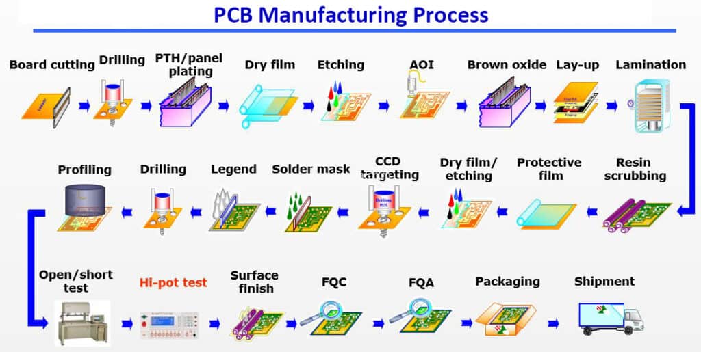
PCB Fabrication Process
The process of manufacturing a 4-layer PCB using KiCAD involves several steps. The first step is to create the PCB layout using the KiCAD software. Once the layout is complete, the next step is to generate Gerber files and drill files. These files are then sent to a PCB manufacturer, who uses them to create the physical PCB.
The PCB fabrication process typically involves several steps, including drilling, plating, and etching. The manufacturer will start by drilling holes in the PCB, which will be used to connect the different layers of the board. The holes are then plated with copper to create a conductive pathway between the layers. Finally, the excess copper is etched away to create the final PCB.
PCB Assembly Process
Once the PCB is fabricated, the next step is to assemble the components onto the board. This process involves placing the components onto the board and soldering them in place. The assembly process can be done manually or using automated equipment, depending on the volume of PCBs that need to be assembled.
The PCB assembly process typically involves several steps, including solder paste application, component placement, reflow soldering, and inspection. The solder paste is applied to the board using a stencil, and the components are placed onto the board using pick-and-place machines. The board is then heated in a reflow oven to melt the solder and create a permanent connection between the components and the board.
Cost Considerations
The cost of manufacturing a 4-layer PCB using KiCAD will depend on several factors, including the size of the board, the number of components, and the complexity of the design. The cost of PCB fabrication and assembly can vary widely depending on the manufacturer and the volume of PCBs that need to be produced.
It is important to consider the cost of manufacturing when designing a PCB using KiCAD. Designers should aim to create a design that is both functional and cost-effective. This can be achieved by minimizing the number of components, optimizing the layout, and selecting components that are readily available and affordable.
In conclusion, manufacturing a 4-layer PCB using KiCAD involves several steps, including PCB fabrication and assembly. Designers should consider the cost of manufacturing when creating a PCB design, and aim to create a design that is both functional and cost-effective.
