EasyEDA is a web-based software that is used for designing electronic circuits and printed circuit boards (PCBs). It is a user-friendly tool that is suitable for beginners and professionals alike. The software allows users to design schematics, PCB layouts, and even simulate circuits before they are built.
One of the most popular features of EasyEDA is its keyboard PCB design capabilities. With EasyEDA, users can easily design their own custom keyboards, including the layout, key switches, and even the case. The software provides a wide range of keyboard components and templates that can be easily customized to fit any design.
EasyEDA’s keyboard PCB design capabilities have made it a popular choice among keyboard enthusiasts and DIYers. The software’s intuitive interface and powerful features make it easy to create high-quality, professional-grade keyboard designs. Whether you are a seasoned keyboard designer or just starting out, EasyEDA is an excellent tool for creating custom keyboards that meet your specific needs.
Designing an EasyEDA Keyboard PCB
Choosing the Keyboard Layout
Before designing an EasyEDA keyboard PCB, it is essential to choose the keyboard layout that best suits your needs. There are various keyboard layouts available, such as ANSI, ISO, and JIS. It is essential to research and choose the layout that best suits your needs.
Creating the Schematic
Once the keyboard layout is chosen, the next step is to create the schematic. EasyEDA provides a user-friendly interface to create schematics. It is essential to place the components accurately and ensure that the connections are correct.
Placing Components
After creating the schematic, the next step is to place the components on the PCB. It is essential to place the components in a way that minimizes the length of the traces and reduces the chances of interference.
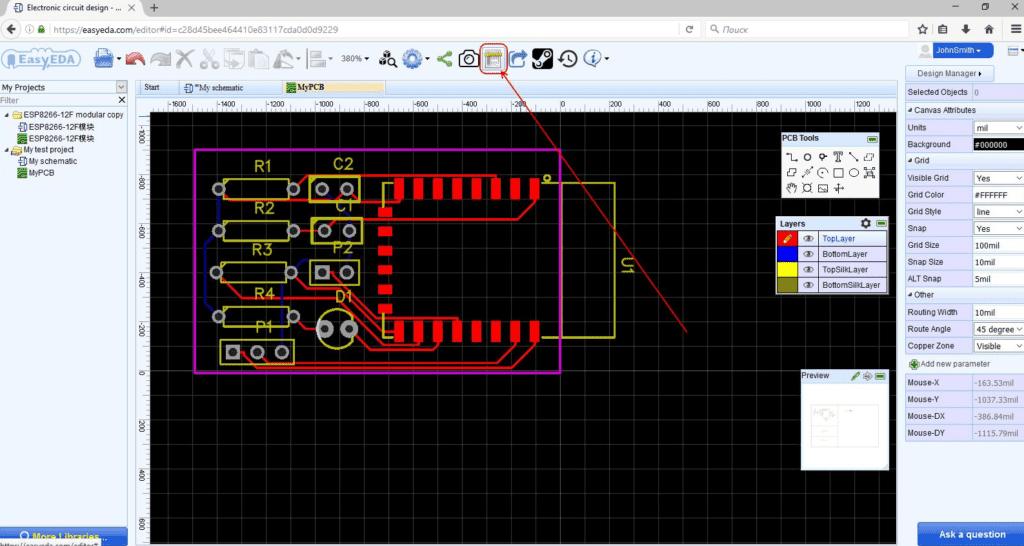
Routing the PCB
Once the components are placed, the next step is to route the PCB. EasyEDA provides a user-friendly interface to route the PCB. It is essential to ensure that the traces are of the correct width and that there are no overlaps or short circuits.
Adding Silk Screen and Copper Pour
After routing the PCB, the next step is to add Silk Screen and Copper Pour. The Silk Screen helps in identifying the components, and the Copper Pour helps in reducing the noise and interference.
In conclusion, designing an EasyEDA keyboard PCB requires careful planning and attention to detail. By following the above steps, one can design a high-quality keyboard PCB that meets their needs.
Manufacturing the EasyEDA Keyboard PCB

Ordering the PCB
To manufacture the EasyEDA Keyboard PCB, you will first need to order the PCB from a manufacturer. EasyEDA provides an option to order the PCB directly from their platform. You can select the PCB’s size, color, and thickness, and the number of PCBs you want to order. The platform also provides an estimated cost and delivery time.
Preparing the PCB Design for Production
Before submitting the PCB design for production, you need to ensure that it is ready for manufacturing. You can use EasyEDA’s Design Rule Check (DRC) to verify if the design meets the manufacturer’s production requirements. The DRC checks for issues such as minimum trace width, minimum distance between traces, and drill hole size.
Once the design passes the DRC, you can export the Gerber files and submit them to the manufacturer. The Gerber files contain the information required to manufacture the PCB, such as the copper layers, solder mask, and silkscreen.
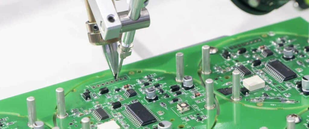
Assembling the Keyboard PCB
Once you receive the PCBs, you can start assembling the keyboard PCB. The assembly process involves soldering the components onto the PCB. You can use a soldering iron and solder wire to solder the components onto the PCB.
Before soldering, ensure that you have the correct components and that they are placed in the correct locations on the PCB. You can use the Bill of Materials (BOM) to verify the components’ values and locations.
Once you have completed the assembly, you can test the keyboard PCB to ensure that it is functioning correctly. You can use a multimeter to test the continuity of the traces and verify that the components are correctly connected.
Overall, manufacturing the EasyEDA Keyboard PCB is a straightforward process that requires careful attention to detail. By following the steps mentioned above, you can create a high-quality keyboard PCB that meets your requirements.
Testing and Troubleshooting the EasyEDA Keyboard PCB
When it comes to testing and troubleshooting the EasyEDA Keyboard PCB, there are a few things you need to keep in mind. In this section, we’ll cover the basics of checking for short circuits and open circuits, testing the keyboard matrix, and debugging common issues.
Checking for Short Circuits and Open Circuits
Before you start testing your EasyEDA Keyboard PCB, it’s important to check for any short circuits or open circuits. Short circuits occur when two or more conductive elements come into contact with each other, while open circuits occur when there is a break in the circuit.
To check for short circuits and open circuits, you can use a multimeter. Set the multimeter to the continuity test mode and place one probe on one end of the circuit and the other probe on the other end. If the multimeter beeps, it means there is continuity, indicating that there is no open circuit. If the multimeter doesn’t beep, it means there is no continuity, indicating an open circuit.
Testing the Keyboard Matrix
Once you’ve checked for short circuits and open circuits, it’s time to test the keyboard matrix. The keyboard matrix is the circuit that connects the keys to the controller. To test the keyboard matrix, you can use a multimeter or a keyboard tester.
To use a multimeter, set it to the continuity test mode and place one probe on one end of the matrix and the other probe on the other end. Press a key on the keyboard and check if the multimeter beeps. If it does, it means the key is working properly. Repeat this process for all the keys on the keyboard.
If you’re using a keyboard tester, simply plug it into the keyboard and press each key. The tester will display the key that was pressed, indicating that it’s working properly.
Debugging Common Issues
If you encounter any issues while testing the EasyEDA Keyboard PCB, there are a few common issues that you can debug. One common issue is ghosting, where pressing one key causes other keys to register as well. This can be caused by a short circuit or a faulty diode. Check for short circuits and replace any faulty diodes to fix this issue.
Another common issue is chattering, where a key registers multiple times with a single press. This can be caused by a faulty switch or a dirty contact. Replace the switch or clean the contact to fix this issue.
Overall, testing and troubleshooting the EasyEDA Keyboard PCB can be a straightforward process if you follow these basic steps.
Conclusion
In conclusion, the EasyEDA Keyboard PCB is a great option for those looking for a customizable and easy-to-use keyboard PCB. With its simple and intuitive interface, users can quickly and easily design and create their own unique keyboard layouts. The platform also provides a wide range of features and tools, including a built-in schematic editor and a powerful PCB layout editor.
One of the major advantages of using EasyEDA Keyboard PCB is its compatibility with a wide range of components and devices. This makes it easy for users to find the parts they need and create their own custom keyboard designs. Additionally, the platform offers a range of templates and examples to help users get started quickly and easily.
Another key benefit of using EasyEDA Keyboard PCB is its affordability. Compared to other similar platforms, EasyEDA offers a range of pricing options that are accessible to both hobbyists and professionals. This makes it a great option for those looking to create their own custom keyboards without breaking the bank.
Overall, the EasyEDA Keyboard PCB is a solid choice for anyone looking for a powerful and user-friendly keyboard PCB design platform. With its range of features, compatibility with a wide range of components, and affordability, it is a great option for both beginners and experienced users alike.
