The EGS002 PCB layout is a crucial component in the design of an inverter for solar power generation. It is responsible for controlling the flow of electricity between the DC input and AC output, ensuring that the power generated by the solar panels is converted into a usable form for home or industrial use. The layout of the EGS002 PCB is critical to the efficiency and reliability of the inverter, making it an important consideration for designers and engineers.
The EGS002 PCB layout is designed to maximize the efficiency of the inverter by minimizing the amount of energy lost during the conversion process. This is achieved through the use of high-quality components and a carefully designed circuit layout that minimizes the resistance of the electrical path. The result is a highly efficient inverter that can convert a large amount of solar power into usable energy for homes and businesses.
Overview
The EGS002 PCB Layout is a popular circuit board design used in various applications. It is designed for use with the SPWM inverter module and is commonly used in motor control and solar power generation systems. In this section, we will provide an overview of the EGS002 PCB Layout and its basics.
EGS002 PCB Layout Basics
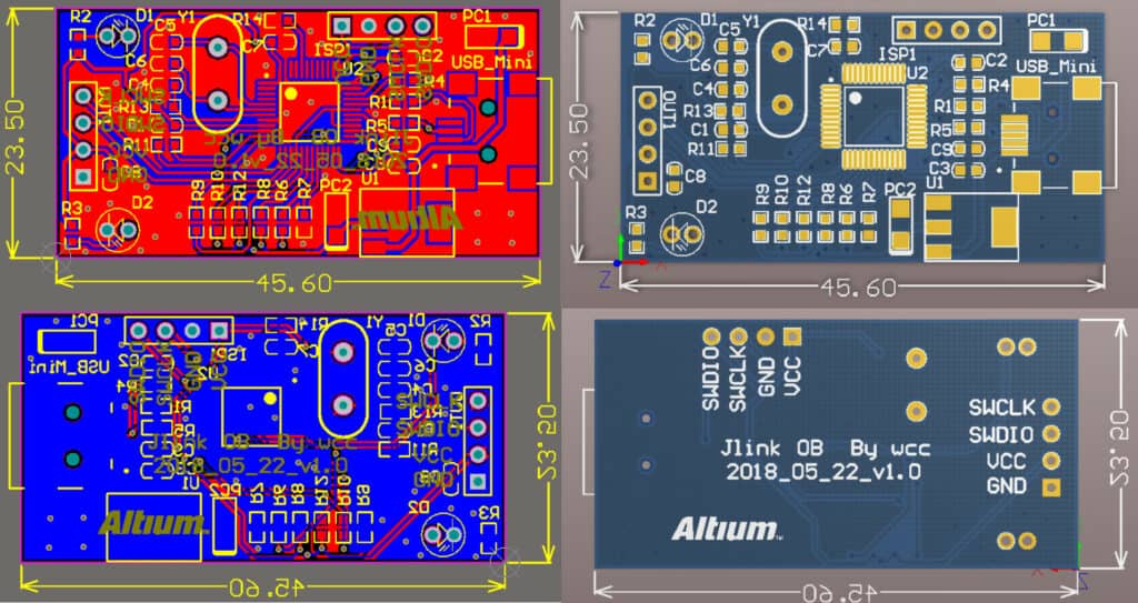
The EGS002 PCB Layout is a double-sided circuit board with a size of approximately 80mm x 50mm. It has a total of 41 components, including resistors, capacitors, diodes, transistors, and ICs. The board is designed to be powered by a DC voltage of 12V or 24V, and it is capable of driving a maximum output power of 1000W.
The EGS002 PCB Layout is designed with a modular structure, which makes it easy to replace or upgrade individual components. The board has a built-in over-current protection circuit that can protect the system from damage in case of a short circuit or overload.
The board has a number of input and output terminals, including the DC power input, the AC output, and the control signal input. The control signal input is designed to be compatible with a wide range of microcontrollers and other control systems, making it easy to integrate into existing systems.
In summary, the EGS002 PCB Layout is a versatile and reliable circuit board design that is widely used in motor control and solar power generation systems. Its modular structure, over-current protection circuit, and compatibility with a wide range of control systems make it a popular choice for many applications.
Design Considerations
When designing the PCB layout for the EGs002, there are several important considerations to keep in mind. These include component placement, signal traces, power traces, and ground plane.
Component Placement
Proper component placement is crucial for optimal performance and reliability of the EGs002. Components should be placed in a logical and organized manner, with consideration for their function and potential interference with other components. It is also important to ensure that components are placed in a way that allows for efficient routing of signal and power traces.
Signal Traces
Signal traces carry the electrical signals between components on the PCB. When designing the signal traces for the EGs002, it is important to keep them as short as possible to minimize signal degradation and interference. Additionally, signal traces should be routed away from noisy components and power traces to avoid any potential interference.
Power Traces
Power traces carry the electrical power throughout the PCB. When designing power traces for the EGs002, it is important to ensure that they are appropriately sized to handle the required current. It is also important to keep power traces as short as possible to minimize voltage drop and power loss.
Ground Plane
The ground plane is an important part of the PCB layout for the EGs002. It helps to reduce noise and interference, and provides a stable reference voltage for the circuit. When designing the ground plane, it is important to ensure that it is connected to all ground pins on the components and that it is not interrupted by signal or power traces.
Overall, careful consideration of component placement, signal traces, power traces, and ground plane is essential for a successful PCB layout for the EGs002. By following these design considerations, you can ensure that your circuit performs optimally and reliably.
Routing Guidelines

Signal Routing
When routing signals, it is important to keep the trace lengths as short as possible to avoid signal degradation and interference. Place critical signals away from noisy components and power traces. Use differential pairs for high-speed signals and keep them as close together as possible. Avoid routing signals over split planes or through vias, as this can cause signal reflection and impedance mismatch. Use wider traces for high-current signals and thinner traces for low-current signals.
Power Routing
When routing power, use wider traces to minimize voltage drop and power loss. Place power traces away from signal traces to avoid noise coupling. Use multiple vias to connect the power planes and distribute the power evenly across the board. Use decoupling capacitors to filter out noise and stabilize the power supply. Place the capacitors as close as possible to the power pins of the components.
Ground Routing
When routing ground, use a solid ground plane to minimize noise and interference. Use multiple vias to connect the ground planes and reduce ground loops. Place ground vias near the components to reduce the ground impedance and improve the grounding. Use star grounding to minimize noise coupling and improve the signal integrity. Avoid routing high-speed signals over the ground plane, as this can cause crosstalk and EMI.
In summary, when routing PCBs for the EGS002, it is important to consider the signal, power, and ground routing guidelines to ensure optimal performance and reliability. By following these guidelines, you can minimize noise, interference, and signal degradation, and improve the overall quality of the design.
PCB Layout Tools

When designing a printed circuit board (PCB), using the right tools is crucial to ensure a successful outcome. There are two main categories of tools that are used in PCB layout: software tools and hardware tools.
Software Tools
PCB layout software tools are essential for designing and creating the actual layout of the PCB. These tools allow designers to create a schematic and then translate that schematic into a physical PCB layout. Some popular software tools for PCB layout include:
- Altium Designer
- Eagle PCB Design
- KiCAD
- OrCAD PCB Designer
- PADS PCB Design
Each of these software tools has its own strengths and weaknesses, so it’s important to choose the one that best fits your specific needs and requirements.
Hardware Tools
In addition to software tools, there are also a variety of hardware tools that can be used in PCB layout. These tools include items such as:
- PCB drill presses
- Soldering irons
- Multimeters
- Oscilloscopes
- Logic analyzers
These hardware tools are used in various stages of the PCB design and manufacturing process, from drilling holes in the PCB to testing the final product.
It’s important to note that while hardware tools are important, they are not as essential as software tools when it comes to PCB layout. Software tools are necessary for creating the layout and ensuring that the design is functional, while hardware tools are used to build and test the final product.
In conclusion, using the right PCB layout tools is crucial for creating a successful design. By using a combination of software and hardware tools, designers can ensure that their PCBs are functional, reliable, and meet their specific requirements.
