Electronic layout design is a crucial aspect of modern electronics manufacturing. It involves the creation of a detailed schematic diagram that maps out the various components, connections, and pathways that make up an electronic circuit. This diagram serves as the blueprint for the physical layout of the circuit on a printed circuit board (PCB), which is essential for the proper functioning of the final product.
The process of electronic layout design requires a deep understanding of the underlying principles of electronics, as well as a high level of technical expertise and attention to detail. Designers must carefully consider factors such as the size and shape of the PCB, the placement and orientation of components, and the routing of electrical signals to ensure that the circuit functions as intended. In addition, they must take into account factors such as heat dissipation, electromagnetic interference (EMI), and signal integrity to ensure that the circuit operates reliably and efficiently.
Overview of Electronic Layout Design
Definition of Electronic Layout Design
Electronic layout design is the process of arranging electronic components, such as resistors, capacitors, and integrated circuits, on a printed circuit board (PCB). The goal of electronic layout design is to create a functional and reliable circuit board that meets the requirements of the electronic device it will be used in.
Importance of Electronic Layout Design
Electronic layout design is a critical step in the development of electronic devices. A well-designed layout can improve the performance, reliability, and manufacturability of a circuit board. A poorly designed layout can result in signal interference, power loss, and other issues that can compromise the functionality of the device.
To ensure a successful electronic layout design, it is important to consider factors such as component placement, signal routing, power distribution, and thermal management. By carefully considering these factors, designers can create a layout that meets the requirements of the device while minimizing the risk of issues such as signal crosstalk, electromagnetic interference, and thermal stress.
In summary, electronic layout design is a crucial step in the development of electronic devices. By carefully considering the various factors involved, designers can create a layout that is both functional and reliable, ensuring the success of the device in the marketplace.
Key Elements of Electronic Layout Design
Circuit Board Layout
Circuit board layout is a critical aspect of electronic layout design. It involves the placement of electronic components and the routing of electrical connections. The layout must be optimized for the intended function, and the design must be efficient and cost-effective.
To achieve an optimal circuit board layout, it is essential to consider factors such as signal integrity, power distribution, thermal management, and electromagnetic compatibility. The layout should also be designed to minimize noise and signal interference.
Component Placement
Component placement is another key element of electronic layout design. The placement of components affects the performance and reliability of the circuit board. Proper component placement ensures that the circuit board is compact, efficient, and reliable.
When placing components, it is essential to consider factors such as signal routing, thermal management, and mechanical stability. The placement of components should also be optimized for signal integrity and electromagnetic compatibility.
Routing
Routing is the process of connecting electronic components on a circuit board. It involves the design of electrical connections that carry signals and power between components. Proper routing ensures that the circuit board functions correctly and is reliable.
When routing, it is essential to consider factors such as signal integrity, power distribution, and thermal management. The routing should also be optimized for electromagnetic compatibility and noise reduction.
In conclusion, electronic layout design is a complex process that requires careful consideration of various factors. The key elements of electronic layout design include circuit board layout, component placement, and routing. By optimizing these elements, designers can create efficient, reliable, and cost-effective electronic circuits.
Tools and Software for Electronic Layout Design

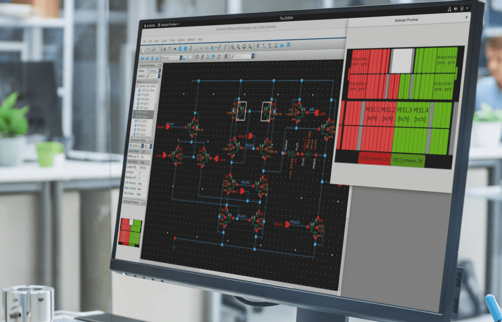
CAD Tools
CAD (Computer-Aided Design) tools are essential for electronic layout design. They allow designers to create, modify, and optimize electronic circuits in a virtual environment before they are physically built. Some popular CAD tools for electronic layout design include:
- Altium Designer
- Eagle PCB Design
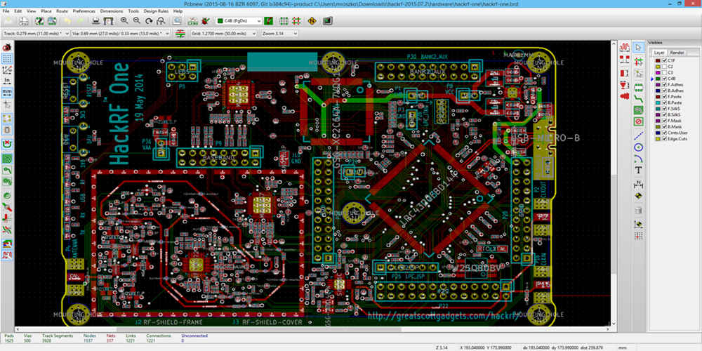
- KiCAD
- OrCAD PCB Designer
- PADS PCB Design
These tools offer a range of features, from schematic capture to 3D visualization, and are suitable for both hobbyists and professionals.
Simulation Software
Simulation software is used to test electronic circuits before they are built. It allows designers to simulate real-world conditions and analyze the behavior of the circuit under different scenarios. Some popular simulation software for electronic layout design include:
- LTspice
- Proteus
- PSpice
- Simulink
- TINA-TI
These tools offer a range of simulation models, from basic analog circuits to complex mixed-signal systems, and are suitable for both beginners and experts.
Design Rule Checkers
Design rule checkers are used to verify that electronic circuits meet specific design rules and constraints. They help to ensure that the circuit is manufacturable and meets the required performance specifications. Some popular design rule checkers for electronic layout design include:
- CAM350
- DFMPro
- HyperLynx DRC
- Valor NPI
- Xpedition DRC
These tools offer a range of design rule checks, from electrical and manufacturing rules to signal integrity and thermal constraints, and are suitable for both PCB designers and manufacturers.
In conclusion, CAD tools, simulation software, and design rule checkers are essential for electronic layout design. They help designers to create, optimize, and verify electronic circuits in a virtual environment, reducing the time and cost of physical prototyping.
Best Practices for Electronic Layout Design
Design for Manufacturability
Design for Manufacturability (DFM) refers to the process of designing a product in a way that makes it easier to manufacture. Here are some best practices for DFM in electronic layout design:
- Use standard components whenever possible to reduce the need for customization.
- Keep the layout simple and avoid complex shapes or angles that can be difficult to manufacture.
- Minimize the number of layers in the board to reduce production time and cost.
- Use a consistent pad and via size to reduce the need for tool changes during production.
Design for Testability
Design for Testability (DFT) refers to the process of designing a product in a way that makes it easier to test. Here are some best practices for DFT in electronic layout design:
- Use test points to make it easier to access and test components.
- Use a consistent naming convention for components to make it easier to identify them during testing.
- Ensure that components are placed in a way that allows for easy access during testing.
- Use design rules to ensure that the board meets the required testability standards.
Signal Integrity
Signal integrity refers to the ability of a signal to travel through a circuit without distortion or loss. Here are some best practices for signal integrity in electronic layout design:
- Use a consistent trace width and spacing to ensure that signals are not affected by crosstalk or noise.
- Keep traces as short as possible to reduce the likelihood of signal degradation.
- Use a ground plane to reduce the risk of electromagnetic interference (EMI).
- Use decoupling capacitors to reduce voltage fluctuations and noise.
By following these best practices for electronic layout design, you can create a product that is easier to manufacture, test, and maintain, while also ensuring that signal integrity is maintained throughout the circuit.
Future of Electronic Layout Design
Emerging Technologies
Electronic layout design is an ever-evolving field that has seen numerous technological advancements over the years. With the increasing demand for more efficient and compact electronic devices, the future of electronic layout design is set to be even more exciting. Here are some emerging technologies that will shape the future of electronic layout design:
- Artificial Intelligence (AI) – AI is set to revolutionize the electronic layout design process by automating many of the tasks that are currently performed manually by designers. AI will enable designers to create more complex designs in less time, resulting in faster time-to-market and improved product quality.
- 3D Printing – 3D printing is already being used in electronic layout design to create prototypes and small-scale production runs. In the future, 3D printing is expected to become more widely adopted, enabling designers to create complex, custom-designed electronic components that are not currently possible using traditional manufacturing methods.
- Flexible Electronics – Flexible electronics are already being used in wearable devices and other applications. In the future, flexible electronics will become even more prevalent, enabling designers to create electronic devices that are more comfortable to wear and easier to integrate into everyday life.
Industry Trends
In addition to emerging technologies, there are also several industry trends that are shaping the future of electronic layout design. Here are some of the most important trends to watch:
- Miniaturization – The demand for smaller and more compact electronic devices is driving the trend towards miniaturization. Designers will need to find ways to pack more functionality into smaller spaces while maintaining high levels of performance and reliability.
- Integration – The trend towards integration is driving the need for more complex electronic layouts that incorporate multiple functions and components into a single device. This trend is being driven by the need for more efficient and cost-effective electronic devices.
- Sustainability – The trend towards sustainability is driving the need for electronic devices that are more energy-efficient and environmentally friendly. Designers will need to find ways to reduce the environmental impact of electronic devices while maintaining high levels of performance and functionality.
Overall, the future of electronic layout design is set to be exciting and challenging. With the emergence of new technologies and the adoption of new industry trends, designers will need to stay up-to-date with the latest developments in order to remain competitive in this rapidly evolving field.
