FM transmitter PCB layout is an essential aspect of designing a high-quality FM transmitter. The proper layout of the printed circuit board can significantly impact the performance and stability of the transmitter. A well-designed PCB layout can minimize interference, reduce noise, and improve the overall signal quality.
To achieve optimal performance, it is crucial to consider several factors when designing an FM transmitter PCB layout. These factors include the placement of components, the routing of traces, and the use of ground planes. Proper component placement can help reduce noise and interference, while careful trace routing can minimize signal loss and distortion. Additionally, the use of ground planes can help reduce noise and improve the overall stability of the circuit.

FM Transmitter PCB Layout Design
When designing an FM transmitter PCB layout, there are several important considerations to keep in mind. These include schematic design, component placement, and routing. By following these guidelines, you can ensure that your FM transmitter will function properly and efficiently.
Schematic Design
The first step in designing an FM transmitter PCB layout is to create a schematic diagram. This diagram will serve as a blueprint for the layout of the PCB. It should include all of the necessary components and connections, as well as any relevant specifications or requirements.
When creating a schematic diagram, it is important to keep it organized and easy to read. Use clear and concise labels for all components and connections, and avoid cluttering the diagram with unnecessary information. This will make it easier to translate the schematic into a physical PCB layout.
Component Placement
Once the schematic diagram is complete, the next step is to place the components on the PCB. Component placement is critical to the overall performance of the FM transmitter, as it can affect signal quality, interference, and other factors.
When placing components, it is important to consider their size, shape, and orientation. Larger components should be placed at the edges of the PCB to avoid crowding, while smaller components can be placed closer together. Components that generate heat, such as transistors or voltage regulators, should be placed away from sensitive components to avoid interference.
Routing
The final step in designing an FM transmitter PCB layout is to route the connections between components. This involves creating a network of traces that connect the various components and carry the signal from the transmitter to the antenna.
When routing connections, it is important to keep the traces as short and direct as possible. This will minimize interference and signal loss. It is also important to avoid crossing traces, as this can create interference and affect signal quality.
By following these guidelines for schematic design, component placement, and routing, you can create an efficient and effective FM transmitter PCB layout. With careful planning and attention to detail, you can ensure that your transmitter will perform reliably and consistently.
PCB Layout Considerations

When designing an FM transmitter, the PCB layout is an important consideration. A well-designed layout can help ensure optimal performance and reliability. Here are some key considerations to keep in mind when designing the PCB layout for your FM transmitter.
RF Design Considerations
When designing the RF section of the PCB, it is important to keep the following considerations in mind:
- Keep the RF traces as short as possible to minimize losses and interference.
- Use a ground plane to provide a low impedance ground and reduce noise.
- Keep the RF components away from other components, especially digital components, to avoid interference.
- Use high-quality components with low parasitic capacitance and inductance to minimize losses and improve performance.
Power Supply Design Considerations
The power supply section of the PCB is critical for reliable operation. Here are some key considerations to keep in mind:
- Use a dedicated power supply for the RF section to minimize noise and interference.
- Use high-quality capacitors and inductors to filter out noise and provide a stable power supply.
- Keep the power supply traces as short as possible to minimize losses and interference.
- Use a ground plane to provide a low impedance ground and reduce noise.
Signal Integrity Considerations
When designing the signal path on the PCB, it is important to keep the following considerations in mind:
- Use a ground plane to provide a low impedance ground and reduce noise.
- Keep the signal traces as short as possible to minimize losses and interference.
- Use high-quality components with low parasitic capacitance and inductance to minimize losses and improve performance.
- Use shielding to protect the signal path from interference.
By keeping these considerations in mind, you can design a PCB layout that will help ensure optimal performance and reliability for your FM transmitter.
PCB Layout Tools
When it comes to designing a PCB layout for an FM transmitter, there are several software tools available in the market. Here are some of the popular ones:
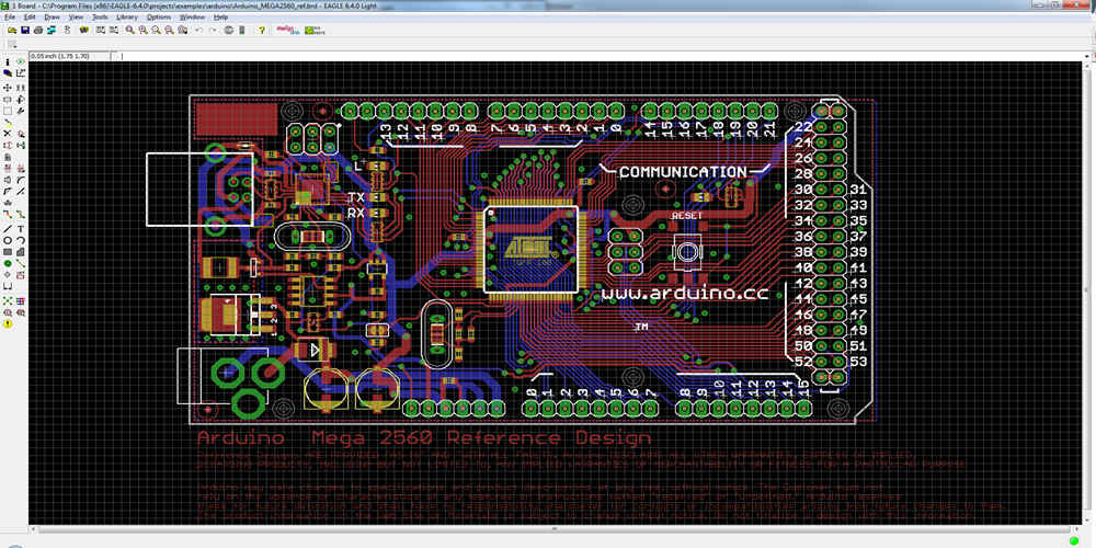
Eagle PCB Design Software
Eagle PCB Design Software is a widely used tool for designing PCB layouts. It offers a user-friendly interface and a vast library of components that can be easily dragged and dropped onto the design canvas. Eagle also offers a range of features, including schematic capture, autorouting, and 3D visualization. The software is available in both free and paid versions.
Altium Designer
Altium Designer is a high-end PCB design software that offers advanced features such as real-time 3D visualization, differential pair routing, and signal integrity analysis. It also has a vast library of components and templates that can be easily customized. Altium Designer is a paid software, and its pricing varies based on the license type.
KiCAD
KiCAD is an open-source PCB design software that offers a range of features, including schematic capture, 3D visualization, and Gerber file generation. KiCAD has a user-friendly interface and is available for free. It also has a vast library of components, and users can create their own components and footprints.
In conclusion, there are several PCB design software tools available in the market, and the choice of tool depends on the user’s requirements and budget. Eagle PCB Design Software, Altium Designer, and KiCAD are some of the popular tools used for designing PCB layouts for FM transmitters.
