High density interconnect boards, popularly known as HDI PCBs are becoming more popular in the electronics industry. These boards offer high performance and are specially designed for some specific applications. Modern devices are becoming more compact and also the components in these devices are becoming smaller. The invention of the HDI circuit board has contributed to this development.
HDI PCB design and manufacturing began in 1980. Then, researchers needed to investigate how to minimize the via size in printed circuit boards. Since then, manufacturers and designers have looked for ways to populate a single board with more components and functions.
What is HDI PCB?
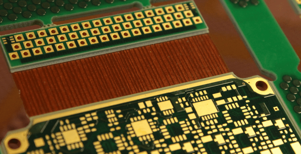
High density interconnect (HDI) PCB is type of circuit board with higher wiring density for each unit surface area. This density is more than that of a standard board. Also, HDI boards have finer lines and space. They comprise minor vias which can capture pads.
HDI board integrates minimum layers and thin materials for its composition. Therefore, these help to enhance its efficiency and performance. HDI PCB layout is suitable for complex designs. Also, HDI boards offer a lot advantages. These boards enhance electrical performance and reduce the size and weight of equipment.
The vias in HDI PCBs are equal to or less than 150 micrometers. Also, the spaces and lines in these boards are equal to or less than 100 micrometers. All these contribute to the reduced size of HDI boards. Furthermore, the increased interconnection density of HDI PCBs helps to improve signal strength and as well increase reliability. HDI PCBs integrate ultra thin materials and very minimum layers compared to standard PCBs.
HDI PCBs contributed to the development of more powerful and smaller electronic devices. When the lines on a circuit become much smaller than 65 microns, therefore, the possibility to etch your space and trace reduces. For instance, etching on a standard PCB enables a thick resist and there are much spaces for tolerances to etch those spaces.
Difference between HDI PCBs and Standard PCBs
HDI technology is a perfect choice for PCB designers when higher density of components is required. Therefore, HDI PCBs are different from standard PCBs based on three reasons.
Microvias replace through hole vias in HDI PCBs
Rather than through hole vias, HDI technology integrates microvias since there is a need for higher precision. Also, laser drilled microvias can create hole depth of about 100μm. Mirovias feature a short bareel and as such, they don’t have problems with various CTE values. Therefore, this makes microvias a more suitable option for HDI boards.
HDI PCB manufacturers replace through holes, blind, or buried vias with microvias to achieve an efficient HDI.
Layer stackup eliminate through hole vias
HDI PCB manufacturing involves different stack-up arrangements. This helps to minimize the number of through-holes and inner layer numbers. Also, the power and ground planes are commonly used to drill vias. Therefore, HDI PCB designers place these layers at the stackup’ s top to minimize the number of stackups.
Arrangement of vias to enhance routing
Via arrangement is very important in HDI PCB design. Also, this arrangement helps to offer enhanced signal integrity.
Laser drilling
HDI printed circuit board integrates laser drilling. This allows the drilling of the smallest microvias which enables more technology on the PCB surface.
Why is HDI PCB Important in Electronic Manufacturing?
There are various benefits of HDI technology. First of all HDI technology helps to reduce the size of devices due to the high connection pad density. Also, HDI PCBs enhance performances of devices. HDI technology contributes to the manufacturing of wearable electronics, handheld electronic devices, and smartphones. Furthermore, the ability to integrate more components in electronics makes HDI PCBs are preferred option among manufacturers.
Smaller weight and size
HDI PCBs enable the production of smaller devices. This is because these boards allow the integration of more components. With reduced board size, manufacturers can build devices that can fit into smaller spaces.
Enhanced signal transmission
High density PCB enhances signal transmission. Also, these boards improve signal quality in electronic devices.
Denser trace routing
HDI PCBs enable manufacturers to integrate more components on the circuit board. This enables denser trace routing. Also, HDI PCB design offers more freedom to freedom to integrate more components on both sides of the board.
High reliability
HDI PCBs are very reliable as a result of its integration of stacked vias. Also, HDI boards offer great protection against any extreme environmental conditions.
Cost effective
HDI technology offers cost effective solutions for electronics production. Quality is a crucial factor when designing electronics. HDI design makes it possible to minimize a standard 8 layer PCB to a 4 layer HDI PCB through the use of microvia. Also, a well-designed 4 layer HDI PCB can offer better functions more than an 8 layer standard PCB.
HDI PCB Design Considerations
Use of microvias
The use of microvias can help PCB designers to achieve more number of pins. Also, microvias can create the escape area of dense components. Microvias feature low inductance which makes them ideal for high-speed applications. Also, they help to link power planes with decoupling capacitors.
Component selection
An HDI PCB usually comprises SMD and BGA components. Also, it is crucial to choose the pitch/spacing between these pins. Proper spacing between pins helps to define board stack-up and trace widths.
Material selection
This is an important consideration for every PCB design. However, it is a more crucial consideration in HDI PCB design. Selecting the appropriate material is ideal for manufacturability and also meeting electrical requirements.
Thermal management
The IPC-2226 standard points out thermal issues in circuit board. Therefore, it is advisable to refer to this standard to ensure better thermal management. Also, designer needs to prevent these thermal issues. Thinner dielectrics can ensure thermal dissipation. It is advisable you add thermal vias to increase dissipation.
Testing
Rather than using In-circuit testing, HDI PCB designers integrate JTAG or functional testing. This is because in-circuit testing usually requires full nodal analysis.
Vias capping
It is advisable you cap or fill microvias to offer a planar surface. Also, capping of vias enables designers to place active parts on the two sides of the PCB. Failure to cap your vias can cause air bubbles and this will affect the quality of solder joint.
Minimized plane perforation
Bigger ground or power copper are enhances power integrity and electromagnetic compatibility. However, microvias create a small gap wherever they perforate a plane and this can have effects on power integrity, signal integrity, and electromagnetic compatibility. Therefore, perforate less to get higher shielding and better image plane effect.
Tips in Achieving Successful HDI PCB Design
HDI board manufacturers must prioritize spacing and layout during HDI PCB design. The tips below will help you achieve a successful HDI PCB design:
Consider spacing
Appropriate spacing is always crucial during HDI PCB design. This means there should be enough space to take many components. Also, it is crucial to leave extra space for components. Before implementation, ensure you consider factors like pad diameter, trace width, and via diameter. Also, you should determine the amount of space needed for components.
Avoid solder-related issues
Solder can result in multiple issues if designers don’t pay attention. For example, via in pads can draw off solder from specific components. This could result in failed connections. The best way to avoid this problem is to integrate via-in-pads. However, this could be impossible due to the PCB design and its applications.
In such cases, the PCB designer needs to use a solder mask to conceal via-in-pads. However, using solder mask can have its own drawbacks. Sometimes, solder mask can have large openings and this can cause solder to get to the PCB. This could further result in disconnected pins. Therefore, it is crucial PCB designers pay apt attention to solder problems before they commence with the design process.
Integrate buried and blind vias wisely
HDI PCB comprises buried and blind vias to maximize limited space. Also, blind vias link outer layers to inner layers. However, they don’t pass through the whole circuit board. On the other hand, buried vias link multiple inner layers without passing through outer layers. Inner layers Buried and blind vias impact the over design of HDI boards. However, designers must be careful with vias as they can impact the construction of PCBs. Also, their placement can affect signal performance.
HDI PCB Fabrication Process
HDI PCB fabrication process involves a lot of steps. Each of these steps must be carefully carried out to achieve a great HDI PCB.
Design
The design is crucial before fabricating your board. Also, you need to be certain that your design matches with the PCB layout. There are a wide range of PCB design software you can use for HDI PCB design.
PCB imaging
The next step after designing your schematic files is PCB imaging. Here, a laser printed film will help you image the PCB. Also, this step helps to achieve ultimate precision and as well provides fine details of the design. After imaging, you will get a photonegative of the HDI PCB you intend to fabricate.
Inner layer printing
This step involves cleaning the laminate. Also, ensure there are no contaminants and dust in the laminate. Also, you will be adding photoresist to the laminate. Photoresist comprises photoreactive chemicals that harden when exposed to ultraviolet rays. Place the films on the pins, this will help to hold the laminate panel.
A blank ink protects the areas that don’t need hardening. After preparing the circuit board, use an alkaline solution to wash the board. This process gets rid of all unhardened photoresist.
Unwanted copper removal
You can remove unwanted copper with a copper solvent solution. In this step, the PCB manufacturer covers the needed copper. Also, you will need to space tracks in case you are making use of heavier copper. Then, use another solvent to wash off any protective layer you used in covering the copper.
Layer alignment
This step deals with the alignment of punches. Also, there are registration holes that enable the alignment of the internal layers with the external layers. You can integrate optical punch for a high level of precision and accuracy.
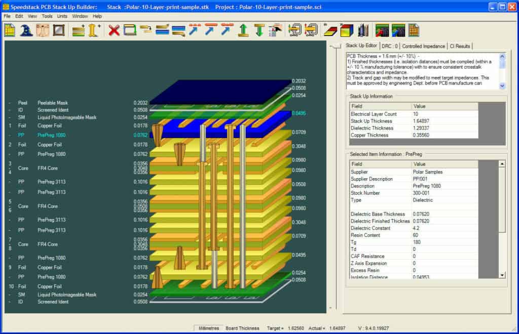
Layering up
In this phase of HDI PCB fabrication process, the manufacturer brings all separate layers together. Also, you will have to fuse these inner layers together. Layer up and bonding are the two primary steps in this phase. Also, the external layer of the PCB comprises fiberglass pre-impregnated with epoxy resin. However, a thin copper foil covers the two sides of the prepreg.
Bonding
Bonding involves fitting the layers in the pins. The prepreg is placed in the alignment basin. After which, a substrate layer goes on top to fit in the copper sheet. Ensure you place another prepreg layer on the copper layer. Also, add copper press plate and aluminum foil.
Laser drilling
Here, you will be creating holes on the stack board with the help of a laser drill. The CO2 will give you a high level of precision. Also, the holes in HDI boards should have very small diameters. This will help to maximize the space on the board. Based on the PCB application, you can create holes with diameters less than 50 μm.
Plating and etching
This step deals with electroplating the PCB panel. Plating helps to get rid of all copper on the board. Etching refers to covering the desired copper with tin. In this step, you will need to remove the remaining copper in the resist layer. Also, this helps to create conductive areas and connections.
Solder mask application
Before applying solder mask, ensure you sanitize the PCB panels. An epoxy solder mask ink will help you achieve this.
Surface finish and silkscreening
There are a wide range of surface finish options to go for. Examples are HASL, immersion gold, and immersion tin. Silkscreening involves specifying the needed information of a board with the use of an inkjet writer.
Electrical testing
Electrical testing is a crucial step in HDI PCB fabrication. It helps to evaluate the consistency and functionality of the PCB.
The Trends and Future of HDI PCB Technology

In life, humans will always demand for changes. Change is a constant thing in life. Constant change, innovation, and development keep happening in the electronics industry. The advent of HDI PCB technology has led to development in electronics manufacturing. Almost all industries benefit from HDI printed circuit board technology.
In the past, printed circuit boards comprise several conductive layers. Things have changed as this is no longer the case. For HDI board technology, the future seems bright. More complex and compact devices will be manufactured. The capability of HDI boards to integrate more components on both sides will make this possible.
Furthermore, blind via and via-in-pad technologies will aid this development. Devices that will be primarily manufactured with HDI circuit boards will transfer signals faster and reduce signal loss. Also, the integration of laser drilling in HDI circuit boards enhances their capabilities. HDI printed circuit boards have fine pitch components.
HDI printed circuit boards minimize the number of conductive layers for a circuit board, thereby reducing dense trace routing. Also, HDI PCBs integrate microvias, buried, and blind vias which enhances routing within a small space. Due to this capability, there is minimized distributing inductance. Hence, this enhances signal integrity.
Also, the HDI PCB technology enabled alternative stack up techniques due to the integration of buried vias, blind vias, and microvias. The integration of drilled sequential lamination has helped manufacturers to increase the density of boards.
HDI has several technological impacts in the PCB industry. One of such is the reduction of the number of layers and size of a board. Therefore, this enhances conductivity.
Crucial Things to Understand in HDI PCB
Microvia Hole
A microvia hole is a blind hole created on the conductor-insulator multilayer. It creates electrical connection via an insulator in the conductive layers.
Minimum pad size hole
The minimum pad size hole on the internal or external layer of an HDI PCB should be +0.010. However, the pad size hole should be +0.014 for the component holes.
Copper wrap
Copper wrap refers to the copper layer that shields the filled holes’ outer surface. Also, the copper wrap’s thickness depends on the outer surface copper thickness of the plated hole.
Recommended via hole plugging
The hole plugging resin always fill the via holes. A permanent hole filling substance will fill this hole.
Capped via hole
The surface’s flatness determines the via in pad design. Also, the holes will be filled with resin. Therefore, you will need an additional thin copper cap.
Factors that Contribute to HDI PCB Cost
There are several factors that affect the cost of HDI PCBs. These factors include:
Type of material
There are different types of PCB material. Also, there are core materials like fiberglass, FR4, and metal. The use of these materials depend on the application. You can integrate surface finishes like immersion tin, ENIG, and HASL. However, ENIG is commonly used for HDI PCBs due to its easy solderability and flatness.
Types of vias
There are different types of vias used in HDI circuit boards. The type of via used in HDI PCB will affect its cost. Also, smaller vias are more expensive than larger vias since they often need more precision. The number of vias present in a HDI PCB can also increase cost.
Number of sequential laminations
Some factors determine the number of sequential laminations in HDI boards. Such factors like number of via structure and number of layers. Although adding more laminations can improve performance, itt could mean more processing which could add to HDI PCB manufacturing cost.
Turnaround time
You may need to pay more if you are in urgent need of your HDI boards. Fast turnaround time often require extra resources and efforts. In some cases, the engineering team will need to work overnight to get your PCB ready.
Use Cases of HDI PCB
HDI PCBs have several use cases. They are popularly used in high performance applications since they offer dense circuitry. Also, they are highly preferred in most industries since they minimize the size of devices.
Military
Military devices work under harsh environmental conditions. Therefore, there is a high demand for high density interconnect (HDI) boards. Military communication devices are usually made from HDI printed circuit boards. Also, you will find a HDI board in military vehicles and jets.
Consumer electronics
The complex and compact consumer electronic devices you see today feature HDI PCB. Also, high density interconnect (HDI) technology has contributed to the development of digital smart phones. These boards have contributed to the advancement in laptops and personal computers. Other electronic devices like LED TVs, touch screen devices, and digital cameras have benefited from HDI printed circuit board.
Most devices in the aerospace industry feature HDI PCBs. Effective heat dissipation in aerospace devices is crucial. Hence, this calls for a higher density interconnect board. HDI circuit board is widely integrated for manufacturing communication and navigation devices in aerospace devices.
Medical
A wide range of medical devices feature HDI printed circuit board. For instance, medical equipment like scanners, colonoscopy camera, and heart monitors comprise HDI boards. Colonoscopy cameras go through the colon of human for examination.
Automotive
The automotive industry is one of the industries that rely on HDI boards. Vehicle manufacturers are highly interested in these boards due to the fact that it enables more innovations. With HDI circuit board, you can save space and as well enhance the performance of a vehicle. Also, vehicles like Tesla integrated HDI PCBs to manage electric functions.
Conclusion
The benefits of HDI PCB technology can’t be overemphasized. It has impacted several industries. Also, this technology creates smaller and lighter electronics while reducing weight and offering substantial space. In addition, the miniaturization of semiconductor packages and components are behind the advancement in this technology.
HDI PCB design requires the consideration of some factors. Revolutionary new devices like wearables, small footprint gadgets, and touch screen computers all integrate HDI PCBs. High density interconnect boards are gradually becoming the mainstay of the electronics industry.
