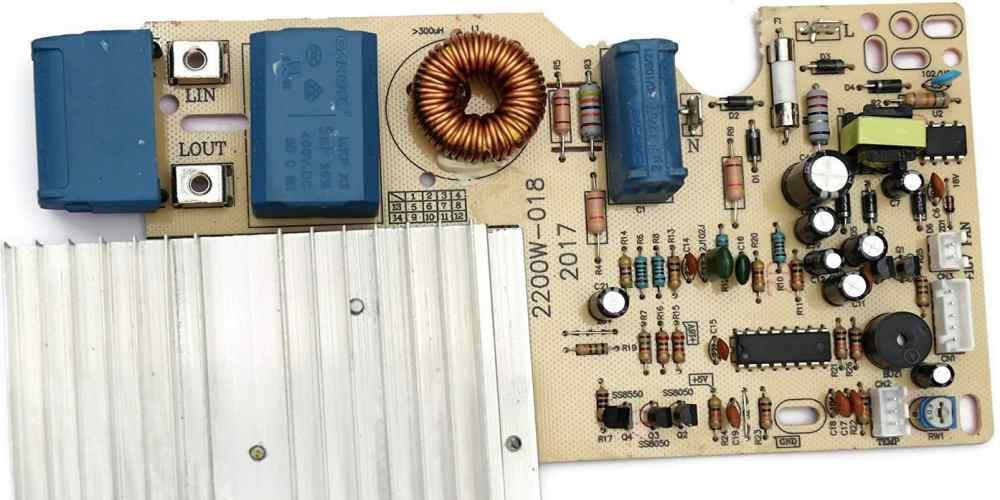
No one can deny the fact that PCBs are integral components of electronic devices. They provide a platform for connecting various electronic components to form a functional circuit. Induction PCBs, aka RF PCBs, are a specialized type of PCB designed to handle high-frequency signals. They have serval uses such as in electronic devices that require wireless communication or operate in high-frequency ranges.
Designers design induction PCBs with specific materials, trace widths, and trace spacing to ensure minimal signal loss and interference. These PCBs have unique features such as grounded planes, stripline transmission lines, and microstrip transmission lines that help to improve signal quality and reduce electromagnetic interference.
The design and manufacture of induction PCBs require expertise in the field of PCB design and manufacturing. The PCB layout and routing must be carefully designed to meet the specific needs of the electronic device. Additionally, the fabrication process of induction PCBs must be precise to ensure accurate trace widths, spacing, and material properties.
Steps for Making of Induction PCBs
1. Choosing the Right Materials
Selecting the right materials is essential for creating high-quality induction PCBs. The choice of materials will depend on the specific requirements of the circuit and the operating frequency range. For example, FR-4 is a common material used for lower frequency PCBs. On the other hand, Rogers or PTFE materials are often good for higher frequency ranges. It is also important to choose materials with low dielectric loss and high thermal conductivity. This will minimize signal loss and heat buildup.
2. Determining Trace Widths and Spacings
Determining the appropriate trace widths and spacings is critical for achieving proper signal performance and reducing electromagnetic interference. This can be a complex process that involves calculating impedance, signal loss, and other factors that affect signal quality. PCB design software can help automate this process. However, it is important to understand the underlying principles to ensure accurate results.
3. Adding Grounded Planes
Grounded planes are essential for reducing electromagnetic interference and improving signal quality in induction PCBs. They help to shield the circuit from external electromagnetic fields. This is how it reduces crosstalk between adjacent signal traces.
4. Creating Stripline and Microstrip Transmission Lines
Stripline and microstrip transmission lines are specialized trace configurations in induction PCBs to transmit high-frequency signals. Stripline transmission lines consist of a signal trace sandwiched between two grounded planes. However, Microstrip transmission lines have signal trace on one layer and a grounded plane on the opposite layer. These trace configurations help to minimize signal loss and interference and ensure consistent signal quality across the circuit.
5. Fabricating the PCB
Once the design is complete, the designers fabricate PCB using either the subtractive or additive process. The subtractive process involves etching away unwanted copper using a chemical solution. On the contrary, the additive process involves depositing copper onto a substrate using electroplating. Both processes have their advantages and disadvantages, and the choice will depend on the specific requirements of the circuit.
6. Assembly and Testing
After the fabrication of PCBs, the designers assemble them onto the board. After this they test the circuit for functionality and performance. Testing can involve measuring signal quality, checking for shorts and opens, and verifying the operation of individual components.
History and Future of Induction PCBs
Induction PCBs have been around for several decades. They have played a vital role in the development of modern electronics. These specialized PCBs allow for the transmission and reception of high-frequency signals. It makes them essential components in many devices, including mobile phones, radar systems, and wireless communication networks. In this section, we’ll look at the history, present, and future advancements of induction PCBs.
The History of Induction PCBs
Induction PCBs have been around since the early days of electronics. However, it wasn’t until the advent of microwave and radar technology during World War II. After that the Induction PCBs began to see widespread use. These early PCBs were relatively simple, consisting of a single layer of copper with a few components.
Later, the advances in material science, design software, and manufacturing techniques enabled the creation of increasingly complex induction PCBs. Today, these PCBs are in wide range of applications, from satellite communication systems to medical devices.
The Current Status of Induction PCBs

In the present day, induction PCBs have become ubiquitous in modern electronics, facilitating wireless communication and high-frequency operation. These PCBs have become increasingly complex and sophisticated. So, it allows more transmission and reception of signals across a wide range of frequencies and bandwidths.
Nowadays, the induction PCBs move towards smaller form factors and higher densities. The demand for smaller and more compact devices has driven the development of miniaturized induction PCBs. These PCBs can fit into increasingly smaller spaces. This has also led to the development of advanced manufacturing techniques. These techniques involve laser drilling and 3D printing, which enable the creation of highly precise and complex PCB designs.
Another important trend in the induction PCBs is the increasing demand for higher frequency and bandwidth capabilities. As devices become more data-intensive, the need for faster and more reliable wireless communication systems has become paramount. This has led to the development of specialized materials, such as Rogers and PTFE. These materials have low dielectric loss and high thermal conductivity, enabling the transmission of high-frequency signals.
Future Advancements in Induction PCB.
Looking towards the future, there are several exciting advancements on the horizon for induction PCBs. One of the key areas of research and development is in the field of nanotechnology. It is a well-known field nowadays which enables the creation of highly precise and efficient PCB designs. Carbon nanotubes and graphene in PCBs can improve thermal and electrical conductivity, reducing signal loss and improving overall performance.
Another area of advancement is in the development of flexible and stretchable PCBs. These specialized PCBs can bend and flex without breaking. This feature has enabled the creation of new and innovative device form factors. Designers are already using the flexible and stretchable PCBs in applications such as smart clothing and medical devices.
Finally, the designers expect that the development of new manufacturing techniques to revolutionize the production of induction PCBs. Advances in 3D printing and laser drilling are enabling the creation of highly precise and complex designs. Furthermore, new materials and techniques for plating and etching are reducing costs and improving efficiency.
What Makes Induction PCBs So Special?
· High-Frequency Capabilities
One of the primary reasons induction PCBs are so famous is their ability to operate at high frequencies. They have designed these PCBs to handle signals in the RF and microwave frequency ranges. These are high frequency signals typically between 100 MHz and 100 GHz. This makes them essential components in several electronic devices, including mobile phones, satellite communication systems, and radar systems.
The ability to handle high-frequency signals is possible due to the construction of induction PCBs. These PCBs have a specialized material, such as Rogers and PTFE. This material has low dielectric loss and high thermal conductivity. This enables the transmission of high-frequency signals with minimal signal loss and interference.
· Miniaturization
Another key advantage of induction PCBs is their ability to be miniaturized. The demand for smaller devices has driven the development of induction PCBs that can fit into increasingly smaller spaces. This is possible by advanced manufacturing techniques, such as laser drilling and 3D printing. These techniques enable the creation of highly precise and complex PCB designs.
The ability to miniaturize induction PCBs has opened new possibilities for the development of innovative devices. These devices include wearable electronics, IoT devices, and medical implants. These devices require highly specialized PCBs that can handle high-frequency signals in a compact and lightweight form factor.
· Reliability and Durability
Induction PCBs are known for their reliability and durability. These specialized PCBs can withstand harsh environmental conditions, including extreme temperatures, humidity, and vibration. This is only because of the use of specialized materials.
The reliability and durability of induction PCBs make them essential components in critical applications. These critical operations are as aviation and medical devices. These applications require PCBs that can operate reliably under extreme conditions without compromising performance or safety.
Induction PCBs are famous for their ability to handle high-frequency signals and their reliability and durability. These PCBs are essential components in many electronic devices and there is increasing use in the future.
Final Note
Induction PCBs are an essential component in modern electronics and communication systems. This is all because of their ability to handle high-frequency signals with minimal signal loss and interference. These specialized PCBs have come a long way since their inception. With new manufacturing techniques they can create highly precise and complex designs.
There will be an increasing use of Induction PCBs as the demand for reliable wireless communication systems increases. Their ability to miniaturize and their reliability and durability make them an attractive option for a wide range of applications. These applications range from wearable electronics and IoT devices to critical applications in aviation and medical devices.
