Creating a PCB design with free and open-source PCB design software is possible with KiCad. The software has no limitations, generates Gerber files, and warns you if something is wrong. It also has a great help center for those just starting.
KiCad is a free and open-source PCB design tool
KiCad is an open-source PCB design tool that lets you design PCBs without wires. It has various features, including a drag-and-drop Components section where you can drag and drop components and join them together, name components, and more. The software also allows you to save designs in various image formats.
After designing your PCB, KiCAD produces the Gerber files needed for manufacturing. These files contain traces and component location information. You can generate Gerber files from your design with KiCAD by selecting the layers of your board and a few other features. After generating the Gerber files, you can send them to the PCB manufacturer.
KiCad’s main aim is to fill the gap left by the lack of high-quality PCB design tools. In addition, its creator, Jean-Pierre Charras, wanted to create a tool to help teach students the principles of electronics and C++. The project started with humble beginnings but has since grown to become a common standard for PCB design in various communities.
Installation is simple. Double-clicking the KiCad installer will start the installation process. If you are using Windows, you can choose to install it through your software manager. The same procedure applies to Linux distros. Once installed, open the software and select a project. To create a new project, click on File > New Project.
The community behind KiCad is an excellent source of help. The developer team and community support each other and even share tutorials, codes, and guides to help speed up the development process. In addition, the open-source nature of the software allows users to expand its capabilities by developing add-ons.
KiCad EDA is free circuit design software that helps designers build and validate designs faster. The program has various features that allow you to design PCBs with ease and accuracy.
It has no limitations
The Kicad PCB design process follows a basic layout. Next, the software will create a footprint for each component based on the schematic. The footprint is a placement guide. Once placed, the footprint will be the appropriate location for the component.
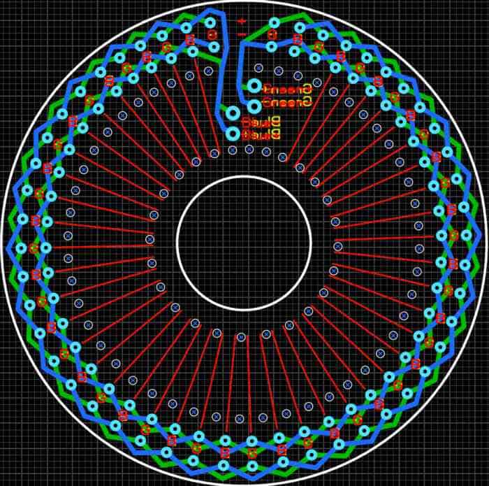
PCBs have multiple layers and a copper zone at the bottom. Various layers sandwich between these layers. Each design layer is a representation of a separate layer of the board. The layers display on the right side of the screen, but this is not necessarily how the PCB will stack up.
Using the Kicad PCB design process is easy and quick. You can generate a drill file, customize design rules, and use default settings. This PCB design software also offers a Design Rules Check feature to ensure that your designs are error-free.
While the KiCad PCB design process is easy to use and intuitive, some users may initially find it difficult to use. However, it is possible to learn KiCad easily if you approach it like a beginner. Remember the famous saying, “Resistance is futile,” which also applies to this software.
KiCad has a thriving community of contributors and users. As a result, the KiCad development team ensures the software continues developing. In addition, the community actively contributes funds to help cover the development costs. For example, a recent fund-raising campaign has raised over sixteen percent of its target amount. This helped guarantee the development of version 6 of the software.
It generates Gerber files
Gerber files are critical for PCB fabrication and assembly. These files contain specifications for components, solder masks, silkscreen pictures, and holes. This data helps manufacturers align their tolerances and layouts on printed circuit boards. It is also necessary for post-assembly electrical testing.
Gerber files are essential for fabrication, so you’ll need to generate them. You can generate them from the PCB design process by clicking on the “File” menu at the top of the screen. Next, select “plot” from the menu. You’ll notice an arrow that indicates which options you can choose. PCBs typically consists of eight layers.
The next step in the PCB design process is to generate Gerber files. These files contain all the design information for the conductor, silkscreen, and solder mask. The process varies with each CAD tool. However, most PCB design software programs generate Gerber files using the RS-274X standard, which superseded the RS-274-D standard. Gerber files are text files and often have a common extension (.gerb).
Before sending your PCB design files to the manufacturer, reviewing them to ensure they are in order is essential. In KiCad, you can check your PCB’s outline layer using the 3D Viewer. If you’ve designed it in manifold mode, you’ll want to ensure the board has no gaps.
Gerber files are a standard format used by PCB manufacturers. They contain information about the physical layers on the PCB. The Gerber files are a standard ASCII vector format; we can open them with any text editor. They contain data and coordinates that are needed to fabricate the PCB.
PCB design software has evolved to be more user-friendly and intuitive to use. KiCad is no exception. The entire process is much easier to learn than many other PCB design tools.
It warns you if there are errors

KiCad uses text-based file formats for its schematic symbols, footprints, and 3D models. The files can be opened with any text-based file-editing software and are compatible with most industry formats, including Gerbers. In addition, its libraries are free and open-source so contributors can add schematic symbols and footprints to the pool. The application also has a huge community of developers around the world.
The XY coordinates are in the bottom information pane. You can duplicate this label to create more than one. The process will warn you if there are any errors during this step. It also uses the Eagle’s knowledge of the parts to detect idiosyncrasies. The current board has seven warnings and no errors.
KiCad also allows you to specify track widths. You can manually input or delete these values or select them automatically. You can also specify custom sizes using the routing tool. KiCad also supports a wide variety of vias.
KiCad’s footprint editor can also help you create footprints for components. These footprints are essential for your PCB design process. The software has thousands of footprints in its library. You can also search online for more footprints.
KiCad has a built-in 3D viewer. It also has many standard libraries for 3D shapes. You can choose from these libraries when you add components to your design. These libraries have default associations for components. You can change them to your preference later.
