Table of Contents
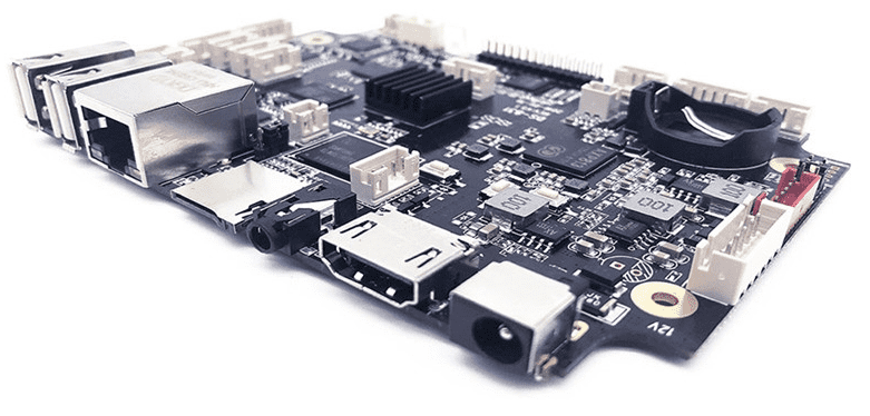
ToggleMobile chargers have become an essential part of our daily lives, keeping our devices charged and ready to use. With the increasing demand for fast and efficient charging, the design of mobile charger printed circuit boards (PCBs) has become crucial. The PCB is the backbone of any electronic device, and a well-designed PCB can significantly improve the performance of a mobile charger.
The design of a mobile charger PCB involves several factors, including the number of charging ports, the type of charging circuit, and the power output. The PCB must be designed to handle the high currents and voltages required for fast charging while ensuring the safety of the user and the device being charged. A well-designed PCB can also help reduce the size and weight of the charger, making it more portable and convenient to use. In this article, we will explore the important considerations in mobile charger PCB design and how they can impact the performance and safety of the charger.

Basics of Mobile Charger PCB Design
Components of a Mobile Charger PCB
A mobile charger PCB typically consists of the following components:
- Transformer: It converts the input AC voltage to a lower AC voltage.
- Rectifier: It converts the AC voltage to DC voltage.
- Filter: It smooths the DC voltage.
- Voltage regulator: It regulates the voltage to a constant value.
- USB port: It provides the output for charging the mobile device.
Design Considerations for a Mobile Charger PCB
Designing a mobile charger PCB requires careful consideration of the following factors:
- Input voltage: The input voltage should match the voltage rating of the transformer.
- Output voltage: The output voltage should be compatible with the mobile device being charged.
- Output current: The output current should be sufficient to charge the mobile device within a reasonable time frame.
- Efficiency: The efficiency of the charger should be high to minimize power loss and reduce heat generation.
- Safety: The charger should be designed to meet safety standards and prevent any potential hazards.
In addition to these factors, the layout of the components on the PCB should be optimized for efficient and reliable operation. Careful consideration should also be given to the selection of components to ensure high quality and long-term reliability.
Overall, designing a mobile charger PCB requires a thorough understanding of the various components and design considerations involved, as well as a commitment to quality and safety.
Mobile Charger PCB Design Process

Schematic Design
The first step in designing a mobile charger PCB is to create a schematic diagram. This diagram represents the electrical connections between the components of the circuit. The schematic design should include all the necessary components, such as the power supply, voltage regulator, USB port, and any other necessary components.
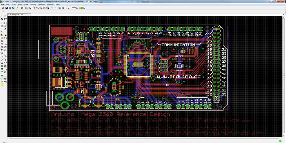
PCB Layout Design
Once the schematic design is complete, the next step is to create a layout design for the PCB. This involves placing the components onto the PCB and routing the electrical connections between them. The layout design must take into account the physical size of the components and the available space on the PCB.
Design Verification
After the PCB layout design is complete, it is important to verify that the design is correct. This can be done by using simulation software to test the circuit and ensure that it is functioning as expected. Additionally, it is important to check the design for any errors or mistakes that may have been made during the design process.
Testing
Once the design has been verified, the final step is to test the PCB. This involves connecting the PCB to a power source and testing the output voltage and current. It is important to ensure that the PCB is functioning correctly and that it is capable of providing the necessary power to charge a mobile device.
In conclusion, the process of designing a mobile charger PCB involves creating a schematic design, laying out the PCB, verifying the design, and testing the final product. By following these steps, it is possible to create a reliable and efficient mobile charger that can be used to charge a variety of different devices.
Advanced Techniques for Mobile Charger PCB Design

Power Management Circuitry
Designing a mobile charger PCB with efficient power management circuitry is essential for ensuring optimal performance and safety. Power management circuitry is responsible for regulating the voltage and current supplied to the battery, preventing overcharging, over-discharging, and short-circuiting.
To achieve efficient power management, designers can use switching regulators, which convert the input voltage to a regulated output voltage with minimal power loss. Additionally, incorporating a charge controller IC can help ensure that the battery is charged at the correct rate and voltage.
Thermal Management Techniques
Thermal management is crucial for preventing overheating and ensuring the longevity of the charger. One effective technique is to use a heat sink, which dissipates heat away from critical components. Another technique is to incorporate thermal vias, which conduct heat away from the PCB and into the surrounding air.
Designers can also use thermally conductive materials, such as copper or aluminum, for the PCB and components. Additionally, incorporating a thermal cutoff switch can help prevent damage to the charger in the event of overheating.
EMI/EMC Considerations
Electromagnetic interference (EMI) and electromagnetic compatibility (EMC) are critical considerations for mobile charger PCB design. EMI can cause interference with other electronic devices, while EMC ensures that the charger does not emit excessive electromagnetic radiation.
To minimize EMI, designers can use EMI filters and shielding, which block or absorb unwanted electromagnetic radiation. Additionally, incorporating a ground plane can help reduce EMI by providing a low-impedance path for electrical currents.
To ensure EMC, designers can use proper grounding techniques, such as star grounding, which minimizes ground loop noise. Additionally, adhering to EMC regulations and standards, such as FCC Part 15 and CISPR 22, can help ensure that the charger meets industry requirements.
Overall, incorporating advanced techniques for mobile charger PCB design can help ensure optimal performance, safety, and compliance with industry standards.
Manufacturing and Assembly of Mobile Charger PCBs
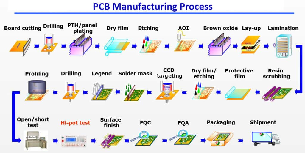
PCB Fabrication Process

The PCB fabrication process is a crucial step in the manufacturing of mobile charger PCBs. The process involves the following steps:
-
Designing the PCB: The first step is to design the PCB using a software tool. The design should be optimized for the specific requirements of the mobile charger.
-
Printing the PCB layout: The next step is to print the PCB layout on a copper-clad board using a laser printer. The printed layout is then transferred to the copper-clad board using heat and pressure.
-
Etching the PCB: The PCB is then etched using a chemical solution to remove the unwanted copper. The remaining copper forms the traces and pads of the PCB.
-
Drilling the PCB: Holes are drilled into the PCB to accommodate the components.
-
Applying the solder mask: A solder mask is applied to the PCB to protect the traces and pads from oxidation and to ensure proper soldering.
-
Applying the silkscreen: The silkscreen is applied to the PCB to provide labeling and component placement information.
Assembly Process
The assembly process involves the following steps:
-
Component placement: The components are placed on the PCB according to the design.
-
Soldering: The components are soldered onto the PCB using a soldering iron or a reflow oven.
-
Testing: The PCB is tested to ensure that it meets the required specifications.
-
Final assembly: The PCB is then assembled into the final mobile charger product.
Overall, the manufacturing and assembly of mobile charger PCBs requires careful attention to detail and precision. The PCB fabrication process and assembly process are critical steps in ensuring the quality and reliability of the final product.

