Panelization is an essential part of the PCB design process, allowing designers to optimize the use of space on a board and reduce manufacturing costs. Altium is a popular software tool used by designers to create PCB designs, and it offers a variety of panelization features to help designers streamline their workflow.
One of the key benefits of panelization in Altium is that it allows designers to place multiple PCB designs on a single panel, which can help reduce the cost of manufacturing. By optimizing the use of space on a panel, designers can produce more PCBs per panel, which can help reduce the cost of materials and labor. Additionally, panelization can help reduce the risk of errors during the manufacturing process, as it allows for more consistent and accurate placement of components.
Another benefit of panelization in Altium is that it allows designers to easily create complex designs that incorporate multiple PCBs. This can be particularly useful for designs that require multiple layers or complex routing, as it allows designers to break up the design into smaller, more manageable pieces. By using panelization in Altium, designers can create more complex designs while still maintaining a high level of accuracy and efficiency.
What is Panelization in Altium?
Panelization is the process of arranging multiple PCB designs onto a single panel for manufacturing purposes. Altium Designer offers a comprehensive panelization feature that allows designers to create and manage panelized PCB designs with ease.
With Altium Designer’s panelization feature, designers can arrange multiple PCB designs onto a single panel in a variety of ways, including:
- Grid-based panelization
- Custom-shaped panelization
- Mixed-panelization
Grid-based panelization is the most common method and involves arranging the PCB designs on a regular grid pattern. Custom-shaped panelization, on the other hand, allows designers to arrange the PCB designs on a non-rectangular panel. Mixed-panelization combines both grid-based and custom-shaped panelization methods.
Altium Designer’s panelization feature also allows designers to add tooling holes, fiducial markers, and other manufacturing-related features to the panelized design. This ensures that the manufacturer can properly align and manufacture the panelized design.
In summary, panelization in Altium Designer is the process of arranging multiple PCB designs onto a single panel for manufacturing purposes. Altium Designer offers a comprehensive panelization feature that allows designers to create and manage panelized PCB designs with ease, including grid-based, custom-shaped, and mixed-panelization methods.
Why is Panelization Important?

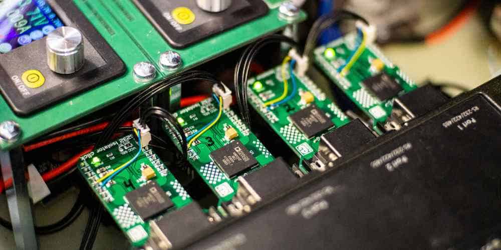
Panelization is an essential step in the PCB manufacturing process that involves grouping multiple PCB designs onto a single panel, which is then fabricated and assembled as a single unit. Panelization offers several benefits that make it a crucial step in the manufacturing process.
Firstly, panelization helps to optimize the use of space on the PCB. By grouping multiple PCB designs onto a single panel, manufacturers can reduce waste and improve efficiency in the manufacturing process. This results in lower costs and faster turnaround times.
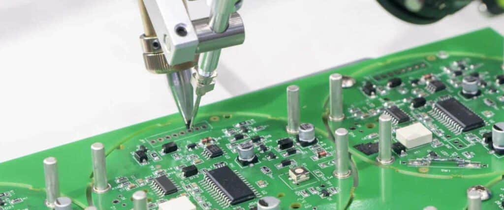
Secondly, panelization makes it easier to handle and transport the PCBs during the manufacturing process. The individual PCBs are held together by a frame, which makes it easier to move them around without damaging them. This is especially important for small PCBs that are difficult to handle individually.
Thirdly, panelization makes it easier to test and inspect the PCBs. By grouping multiple PCBs onto a single panel, manufacturers can test and inspect them as a single unit. This reduces the time and cost associated with testing and inspection.
Finally, panelization helps to ensure the quality of the PCBs. By grouping multiple PCBs onto a single panel, manufacturers can ensure that all of the PCBs are produced to the same high standard. This reduces the risk of defects and improves the overall quality of the final product.
In summary, panelization is an important step in the PCB manufacturing process that offers several benefits, including improved efficiency, easier handling and transport, easier testing and inspection, and improved quality.
How to Panelize in Altium
Creating a New Panel
To create a new panel in Altium, you need to open the PCB file that you want to panelize. Then, go to the Design menu and select Panelize. In the Panelize dialog box, click the New button to create a new panel. You can then specify the size of the panel and the number of copies you want to create.
Adding Components to the Panel
Once you have created a new panel, you can add components to it by dragging and dropping them from the PCB file. You can also add components by using the Add button in the Panelize dialog box. When you add components to the panel, they will be automatically duplicated according to the settings you specified.
Arranging Components on the Panel
After you have added components to the panel, you can arrange them in any way you like. You can move components around by clicking and dragging them, and you can resize them by dragging their edges. You can also use the Align and Distribute tools to align and distribute components on the panel.
Generating the Panelized Output
Once you have arranged the components on the panel, you can generate the panelized output by clicking the Generate Outputs button in the Panelize dialog box. Altium will then create a new PCB file that contains the panelized output. You can then use this file to manufacture the panel.
In summary, panelizing in Altium is a straightforward process that involves creating a new panel, adding components to the panel, arranging components on the panel, and generating the panelized output. With these simple steps, you can easily create a panel that meets your manufacturing needs.
Best Practices for Panelization in Altium
Design Considerations
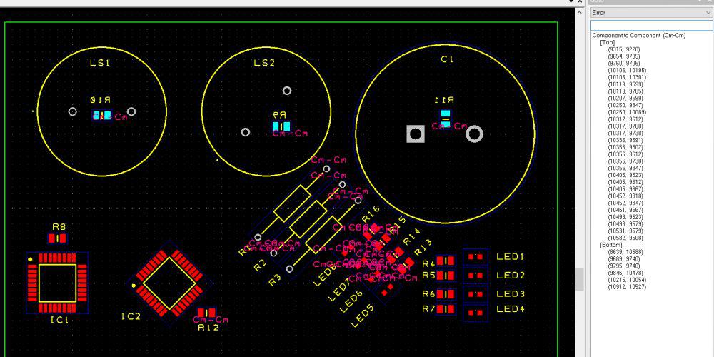
When designing a PCB panel, it’s important to consider the following:
- Panel Size: Determine the panel size based on the manufacturing process and the size of the individual PCBs.
- PCB Layout: Ensure that the PCB layout is optimized for panelization. This includes aligning the components and traces, and leaving enough space between the PCBs for the manufacturing process.
- Panelization Method: Choose the appropriate panelization method based on the manufacturing process and the number of PCBs required.
Panelization Techniques
Altium provides several panelization techniques, including:
- Manual Panelization: Manually arrange the PCBs on the panel.
- Array Panelization: Create an array of identical PCBs on the panel.
- Step-and-Repeat Panelization: Repeat a single PCB layout multiple times on the panel.
- Mixed Panelization: Combine different PCB layouts on the same panel.
Panelization for Manufacturing
When panelizing for manufacturing, consider the following:
- Panelization Guidelines: Follow the manufacturer’s panelization guidelines to ensure that the panel can be manufactured correctly.
- Panelization Markings: Add panelization markings, such as tooling holes and fiducial marks, to the panel to aid in the manufacturing process.
- Panelization Documentation: Include panelization documentation, such as a panel drawing and bill of materials, to ensure that the panel can be accurately reproduced.
By following these best practices, you can ensure that your panelized PCBs are optimized for manufacturing and can be produced accurately and efficiently.
Conclusion
In conclusion, panelization is a crucial step in the PCB design process that can help save time and reduce costs. By grouping multiple PCBs onto a single panel, designers can streamline the manufacturing process and improve the efficiency of their workflow.
Altium offers a range of features and tools to simplify the panelization process, including the ability to define board arrays, add tooling holes, and create custom panel templates. With these tools, designers can easily create professional-quality panels that meet their specific requirements.
When panelizing PCBs, it is important to consider factors such as board size, spacing, and orientation, as well as the requirements of the manufacturing process. By carefully planning and executing the panelization process, designers can ensure that their PCBs are manufactured accurately and efficiently.
Overall, panelization is an essential aspect of PCB design that can help improve the quality and reliability of electronic products. With the right tools and techniques, designers can create high-quality panels that meet their specific requirements and achieve optimal results.
