Printed Circuit Boards (PCBs) are at the heart of modern electronics. They are the backbone of almost every electronic device, from smartphones to computers, and from cars to medical equipment. A PCB is a board made of insulating material, such as fiberglass, with conductive pathways etched onto its surface. These pathways allow electrical signals to flow between different components on the board, enabling the device to function.
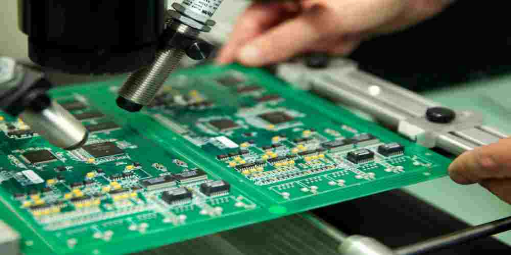
The process of designing a PCB starts with a schematic diagram of the circuit. This diagram shows the various components in the circuit and how they are connected. The schematic is then converted into a layout that can be used to manufacture the board. The layout specifies the placement of components, the size and shape of the board, and the routing of the conductive pathways. Once the layout is complete, the board can be manufactured using a variety of techniques, including etching, milling, or printing. The resulting PCB is then tested to ensure that it functions correctly.
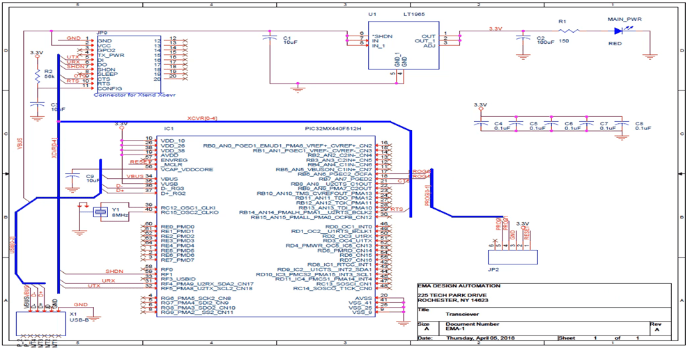
Creating a Schematic
Choosing a PCB Design Software
Before creating a schematic, it is important to choose the right PCB design software. There are various software options available in the market, and one should choose software that meets their needs and budget. Some popular PCB design software options include Altium Designer, Eagle PCB, KiCAD, and Proteus.
Drawing the Schematic
Once the software is selected, the next step is to draw the schematic. A schematic is a graphical representation of the electronic circuit. It shows the components and their connections. The schematic should be drawn in a clear and organized manner so that it is easy to read and understand.
Adding Components to the Schematic
After drawing the schematic, the next step is to add components to it. The components should be selected based on the requirements of the circuit. The software should have a library of components that can be used to add components to the schematic.
Connecting Components in the Schematic
Finally, the components should be connected in the schematic. This involves drawing wires between the components to show how they are connected. The connections should be made in a logical and organized manner so that it is easy to read and understand the schematic.
In summary, creating a schematic is an important step in the PCB design process. It involves choosing the right software, drawing the schematic, adding components, and connecting them. By following these steps, one can create a clear and organized schematic that will serve as the basis for the PCB design.
Generating the Netlist

What is a Netlist?
A netlist is a list of all the electrical connections in a printed circuit board (PCB). It is a critical step in the PCB design process, as it provides the information necessary for the PCB manufacturer to create the physical board. The netlist contains information about each component’s pins, their connections to other pins, and the electrical properties of the connections.
Generating the Netlist from the Schematic
Generating a netlist from the schematic is a simple process that involves exporting the schematic data in a format that can be read by the PCB design software. The netlist is created by assigning unique names to each pin on each component in the schematic, and then creating a list of connections between those pins.
Once the netlist is generated, it can be imported into the PCB design software to create the physical board. The software uses the netlist to create a layout of the board, placing each component in its correct location and routing the connections between them.
It is important to note that the netlist must be generated accurately to ensure that the physical board matches the intended design. Any errors in the netlist can result in a non-functional board or even damage to components.
In conclusion, generating a netlist is a crucial step in the PCB design process. By accurately capturing the electrical connections between components, the netlist ensures that the physical board will function as intended.
Importing the Netlist into PCB Design Software
Choosing the Right PCB Design Software
When it comes to choosing a PCB design software, there are many options available. Some popular software includes Altium Designer, Eagle PCB, and KiCAD. It is important to choose a software that meets your specific needs and budget. Consider factors such as ease of use, compatibility with your schematic software, and available features.
Importing the Netlist into the PCB Design Software
After completing the schematic design, the next step is to import the netlist into the PCB design software. The netlist contains information about the connections between components in the schematic. This information is used to create the physical layout of the PCB.
Most PCB design software has an option to import the netlist directly from the schematic software. The netlist file format may vary depending on the schematic software used. It is important to ensure that the netlist is compatible with the PCB design software being used.
Once the netlist is imported, the software will generate a layout for the PCB. The layout can be modified as necessary to meet the specific requirements of the design. This includes adding components, adjusting component placement, and routing the connections between components.
In conclusion, importing the netlist into the PCB design software is a crucial step in the process of creating a PCB. Choosing the right software and ensuring compatibility between the schematic and PCB design software is important to ensure a successful design.
Laying Out the PCB
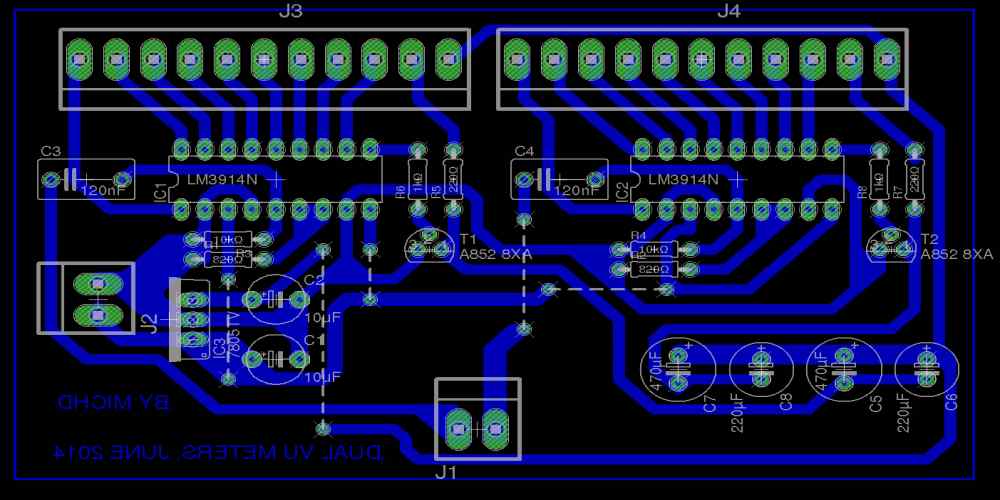
Creating the Board Outline
The first step in laying out a PCB is to create the board outline. This will define the physical dimensions of the board and its shape. The board outline should be created based on the size and shape of the components that will be placed on the board. It is important to ensure that the board outline is large enough to accommodate all the components and that there is enough space between them to allow for routing of the traces.
Placing Components on the Board
Once the board outline has been created, the next step is to place the components on the board. The placement of the components is critical to the performance of the circuit. Components should be placed in a logical and organized manner, taking into account their function and their relationship to other components on the board. It is important to ensure that there is enough space between the components to allow for routing of the traces.
Routing the Traces
After the components have been placed on the board, the next step is to route the traces. Traces are the pathways that connect the components on the board. The routing of the traces is critical to the performance of the circuit. Traces should be routed in a logical and organized manner, taking into account their function and their relationship to other traces on the board. It is important to ensure that the traces are routed in a way that minimizes noise and interference.
Adding Copper Pour
Finally, after the traces have been routed, the next step is to add copper pour. Copper pour is a technique used to fill empty spaces on the board with copper. This helps to reduce noise and interference and also helps to dissipate heat. Copper pour should be added in a logical and organized manner, taking into account the function of the circuit and the relationship between the components on the board.
In conclusion, laying out a PCB is a critical step in the design process. It is important to ensure that the board outline is created based on the size and shape of the components, that the components are placed in a logical and organized manner, that the traces are routed in a way that minimizes noise and interference, and that copper pour is added in a logical and organized manner. By following these steps, you can ensure that your PCB design is optimized for performance and reliability.
Design Rule Check and Gerber Generation
Running a Design Rule Check
Once the schematic is complete, the next step is to create the printed circuit board (PCB) layout. Before generating the Gerber files, it is important to run a Design Rule Check (DRC) to ensure the design meets the manufacturer’s specifications.
A DRC is a software check that verifies the design against a set of rules defined by the manufacturer. These rules may include minimum trace width, minimum clearance between traces, and minimum drill size, among others. Running a DRC ensures that the design is manufacturable and will function as intended.
Most PCB software packages include a DRC tool that can be run before generating the Gerber files. The DRC tool will highlight any errors or violations that need to be corrected before proceeding.
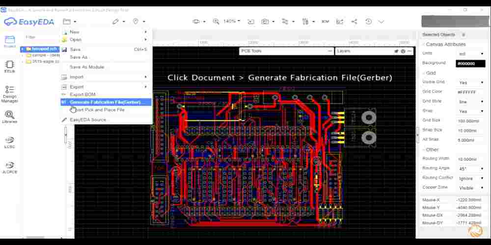
Generating Gerber Files
Once the DRC has been run and any errors have been corrected, the next step is to generate the Gerber files. Gerber files are a standard file format used by PCB manufacturers to create the physical PCB.
To generate Gerber files, the PCB software package will usually have an option to export the design as Gerber files. The software will generate a set of files, each representing a different layer of the PCB. These files will include information about the location of components, traces, and other features on the board.
It is important to check the Gerber files before sending them to the manufacturer to ensure that everything is correct. Most PCB software packages include a Gerber viewer that allows the user to view the files and ensure that they match the intended design.
In conclusion, running a DRC and generating Gerber files are critical steps in the design process of a PCB. By following these steps, designers can ensure that their designs are manufacturable and will function as intended.
Conclusion
In conclusion, designing a Printed Circuit Board from a schematic is a complex process that requires attention to detail and a thorough understanding of the design requirements. Throughout this article, we have discussed the various steps involved in the process, from creating a schematic diagram to generating a PCB layout.
We have seen how important it is to carefully review the schematic diagram and ensure that all components are correctly placed and connected. We have also explored the various software tools available for generating a PCB layout, such as Eagle, Altium, and KiCad.
When designing a PCB, it is important to consider factors such as the size and shape of the board, the location of components, and the routing of traces. By carefully planning the layout and routing of the board, it is possible to minimize noise and interference, and ensure that the board operates reliably.
Finally, it is important to thoroughly test the finished PCB to ensure that it meets the design requirements and performs as expected. This may involve using specialized testing equipment, such as an oscilloscope or logic analyzer.
Overall, designing a PCB from a schematic requires a combination of technical expertise, attention to detail, and careful planning. By following the steps outlined in this article, it is possible to create a high-quality PCB that meets the design requirements and performs reliably.
