PCB CAD layout is a crucial aspect of printed circuit board design. It involves the placement of components and routing of electrical connections on a PCB board. The layout of a PCB can significantly impact the performance and reliability of an electronic device.
One of the primary goals of PCB CAD layout is to minimize signal interference and noise. By carefully arranging components and routing traces, designers can reduce the amount of electromagnetic interference (EMI) and crosstalk between signals. This can help improve signal integrity and reduce errors or malfunctions in the device.
Moreover, PCB CAD layout also plays a significant role in the manufacturability and cost-effectiveness of a PCB design. A well-designed layout can help reduce the number of layers required, simplify the assembly process, and minimize the use of expensive materials. Therefore, it is essential to consider the PCB CAD layout early in the design process to ensure a successful, reliable, and cost-effective product.
Basics
What is PCB CAD layout?
PCB CAD layout is the process of designing the physical layout of a printed circuit board (PCB) using computer-aided design (CAD) software. It involves placing components and routing traces on the PCB to create a functional circuit that meets the design requirements.
Why is PCB CAD layout important?
PCB CAD layout is important because it determines the functionality, reliability, and performance of the final product. A well-designed layout can reduce electromagnetic interference, improve signal integrity, and minimize crosstalk between components. It can also reduce the size and cost of the PCB, while improving its manufacturability and ease of assembly.
How does PCB CAD layout work?
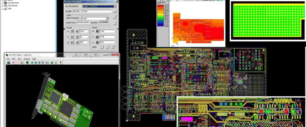
PCB CAD layout involves several steps, including component placement, trace routing, and design rule checking. The process begins with importing the schematic design into the CAD software and placing the components on the PCB. The next step is to route the traces between the components, taking into account factors such as signal integrity, power distribution, and thermal management. Finally, the layout is checked against design rules to ensure that it meets the requirements for manufacturing and assembly.
In summary, PCB CAD layout is a critical step in the design and development of a printed circuit board. It involves using CAD software to design the physical layout of the PCB, taking into account factors such as component placement, trace routing, and design rules. A well-designed layout can improve the performance and reliability of the final product, while reducing its size and cost.
PCB CAD Layout Design Process

The PCB CAD layout design process involves several steps that must be followed to ensure a successful PCB design. These steps include schematic capture, component placement, routing, and design rule checking (DRC).
Schematic Capture
Schematic capture is the first step in the PCB CAD layout design process. It involves creating a schematic diagram of the circuit using a schematic capture tool. The schematic captures the electrical connections between components and serves as a blueprint for the PCB layout.
Component Placement
The next step is component placement. This involves placing the components on the PCB layout in a logical and efficient manner. The placement should take into consideration the size and shape of the components, as well as the electrical connections between them.
Routing
Routing is the process of creating copper traces on the PCB layout to connect the components. The routing should be done in a way that minimizes the length of the traces and reduces the possibility of crosstalk and interference.
Design Rule Checking (DRC)
The final step in the PCB CAD layout design process is design rule checking (DRC). This involves running a DRC tool to check the design against a set of design rules. The DRC tool checks for errors such as short circuits, clearance violations, and trace width violations.
Overall, the PCB CAD layout design process is a critical step in the development of a successful PCB design. By following the steps outlined above and using the appropriate tools and techniques, designers can create high-quality PCB layouts that meet the needs of their applications.
Tools for PCB CAD Layout

When it comes to designing a PCB, having the right tools is essential. Here are two main categories of tools for PCB CAD layout:
Software for PCB CAD Layout
There are several software options available for PCB CAD layout. Some popular options include:
- Altium Designer: This software is widely used in the industry and offers a comprehensive suite of tools for PCB design.
- Eagle PCB Design: This software is popular among hobbyists and small businesses and offers a free version for non-commercial use.
- KiCad: This open-source software is gaining popularity due to its affordability and ease of use.
Each software has its own strengths and weaknesses, so it’s important to research and choose the one that best fits your needs.
Hardware for PCB CAD Layout
In addition to software, there are also hardware tools that can aid in PCB CAD layout. Here are a few examples:
- Mouse: A high-quality mouse can make it easier to navigate through design software and make precise movements.
- Keyboard: A keyboard with customizable hotkeys can make the design process more efficient.
- Monitor: A large, high-resolution monitor can provide a better view of the design and improve productivity.
Again, the specific hardware tools needed will depend on individual preferences and needs.
Overall, having the right tools can make a significant difference in the efficiency and accuracy of PCB CAD layout. By researching and investing in the appropriate software and hardware, designers can create high-quality PCBs that meet their specifications.
Tips for Effective PCB CAD Layout
Keep it Simple
One of the most important tips for effective PCB CAD layout is to keep it simple. Avoid cramming too many components into a small space, as this can lead to signal interference, noise, and other issues. Instead, try to use a simple and straightforward layout that allows for easy routing and testing.
Use Standard Design Rules
Another important tip is to use standard design rules when creating your PCB layout. This ensures that your board will be compatible with other components and devices, and that it will work correctly. Standard design rules also help to ensure that your PCB will be manufacturable, reducing the risk of errors and delays.
Consider Signal Integrity
Signal integrity is a critical factor in PCB design, and it’s important to consider it when laying out your board. Make sure to keep high-speed digital signals away from analog signals, and avoid placing components too close together. Use ground planes and power planes to reduce noise and interference, and consider using impedance-controlled traces for high-speed signals.
Check for Errors
Finally, it’s important to check your PCB layout for errors before sending it off for fabrication. Use a design rule checker to ensure that your layout meets all necessary specifications, and check for errors such as missing connections, incorrect net names, and overlapping components. By catching and fixing errors early on, you can save time and money in the long run.
In summary, effective PCB CAD layout requires a simple and straightforward design, adherence to standard design rules, consideration of signal integrity, and thorough error checking. By following these tips, you can create a high-quality PCB that meets your needs and performs reliably.
Future of PCB CAD Layout
PCB CAD Layout has come a long way since its inception. With advancements in technology, the future of PCB CAD Layout looks bright. Here are some of the developments that we can expect to see in the future:
-
Increased Automation: PCB CAD Layout will become more automated, reducing the time and effort required to design a circuit board. This will be achieved through the use of machine learning and artificial intelligence algorithms.
-
Cloud-based Design: Cloud-based PCB CAD Layout will allow designers to work collaboratively on a project, regardless of their location. This will increase efficiency and reduce the time required to complete a project.
-
3D Printing: The use of 3D printing in PCB CAD Layout will become more common. This will enable designers to create more complex designs and prototypes.
-
Improved Design Tools: The tools used in PCB CAD Layout will become more sophisticated, making it easier for designers to create high-quality designs. This will include better visualization tools, simulation software, and more.
-
Integration with Other Technologies: PCB CAD Layout will become more integrated with other technologies such as the Internet of Things (IoT) and Artificial Intelligence (AI). This will enable designers to create more complex and sophisticated designs.
In conclusion, the future of PCB CAD Layout looks bright with the advancements in technology that we can expect to see. These developments will improve efficiency, reduce the time required to complete a project, and enable designers to create more complex and sophisticated designs.
