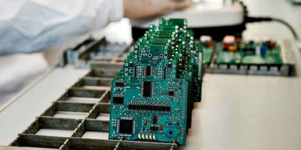
When manufacturers are producing PC boards in bulk, they are more likely to avoid soldering components onto the PCBs manually. Instead, they will utilize professional printed circuit board machines to solder and assemble various components onto the circuit board.
But how do these machines assemble all the small components that you find in a printed circuit board? And is it just one machine that carries out the entire assembly process? Generally, when ordering a printed circuit board, you will want to ensure that the company handling your order is competent. And a significant part to consider when judging a company’s competence is the gadgets they utilize to assemble your PCB. Having some knowledge about how PCB components assembly machines function can help you a lot in making your decision. Moreover, electronic gadgets are becoming more complex by the day. This means that the machinery manufacturers utilize to manufacture them is also becoming more complex and interesting by the day.
PCB Assembly Machines in a Nutshell
In the Printed Circuit Board assembly process, manufacturers mostly go through four crucial stages. These stages are the application of paste, placement of components automatically, soldering, and PCB inspection. Moreover, the manufacturer might also carry out the fifth step, which involves testing the PCB if the need arises.
The primary PCB assembly machines that manufacturer utilize to assemble components onto PCBs includes:
- Solder paste Gadget
- Solder paste Inspection Gadget
- Glue Dispensing Gadget
- Pick-and-place gadget
- Reflow soldering gadget
- Wave soldering gadget (for THT components)
- Automatic Optical Inspection gadgets
Paste Application
The Solder Paste Printing Gadget
Generally, the very first phase in the printed circuit board assembly process involves technicians applying solder paste to the PCB.
Solder paste is typically gray in color, and it encompasses a mixture of multiple metals alloy particle alloys, which include:
- Silver
- Lead
- Tin
You can think of solder paste as an effective glue that technicians utilize on PC boards to hold everything together. Generally, without solder paste, various electro components would not stick to the bare board.
However, technicians must place a stencil over the PCB before applying solder paste. A printed circuit board stencil is a simple sheet of stainless steel with tiny laser-cut holes. The purpose of these laser-cut holes is to help technicians apply the solder in the right places with high precision.
During the solder paste application process, technicians secure the PC board and board stencil in place in the auto-paste printer. After locking the two components in place, the auto-paste printer then utilizes a squeegee that applies the solder paste onto the PCB with great precision in terms of amount and area of application.
After application, the gadget automatically drags a special blade across the PCB stencil to effectively spread the solder paste and deposit it evenly in the right areas. When this process is over, technicians remove the stencil, and the PCB is ready to move to the next phase.
Solder Paste Inspection Gadget
Statistics show that most printed circuit boards with issues after production probably had substandard or improper solder paste application. Actually, over 70% of flawed PCB are due to substandard or inappropriate solder paste application. Therefore, technicians must ensure that the solder application process is perfect to avoid generating erroneous printed circuit boards.
When simply utilizing impeccable solder paste application methods is efficient in terms of ensuring fewer errors during the solder paste application phase. If you are dealing with bulk PCB production, you should highly consider SPI since it helps in terms of assessing high volumes of printed circuit board, and it will help you avoid rework costs which can be a lot.
Generally, the solder paste inspection gadget uses high-quality, complex cameras that capture images in three dimensions. After capturing the image of the PCB in 3D, it evaluates the solder paste’s quality via factors such as:
- Height
- Alignment
- Solder volume
The gadget then effectively points out imperfect alignment or unsuitable solder volumes, allowing technicians to make adjustments quickly before things get out of hand. When manufacturers utilize SPI together with AOI (automated optical inspection), they are able to effectively control and monitor the PCB soldering process. Doing so helps them save them a lot of money, and it also helps them generate high-quality printed circuit boards each time.
Auto Component Placement

Before the component placement process, technicians utilize a glue dispensing gadget to accurately apply tiny dots of glue to the printed circuit board on the exact locations where the electrical components will sit. The adhesive holds the electrical components in place till the contacts and leads are effectively soldered.
The glue application process is particularly crucial if the technicians are utilizing the wave soldering technique to assemble the electrical components. That is because the solder waves might dislodge more significant electrical components from the board.
Pick-and-Place Gadget
Out of all the gadgets you can find in PCB assembly firms, the pick-and-place gadget will probably be the most fascinating machine you will see. Just like the name of this gadget suggests, the pick and place gadget picks up electrical components and then places them on the bare board.
Earlier on, before pick-and-place gadgets hit the market, this process was done manually. Humans were painstakingly picking electrical components and placing them onto the circuit board one by one using tweezers. However, nowadays, PCB manufacturers utilize pick-and-place gadgets to effectively automate this process since machines tend to be more accurate when compared to humans. Moreover, machines can work 24/7 without taking a break which makes them efficient for this task.
Generally, pick and place gadgets suck up surface mount tech components and then place them onto the board on the areas containing solder paste with great precision. However, the pick and place machine utilizes pre-programmed positions to effectively place the components onto the board with great precision. Moreover, the gadget places components in their exact locations on the board pretty fast. Actually, most of these gadgets achieve speeds of around 30,000 electrical components per hour, which is a lot of components compared to when humans carry out this process manually.
The pick-and-place gadgets function in a pretty organized manner which makes them the most mesmerizing gadgets to watch in the PCB assembly process.
Soldering
Reflow Soldering Gadgets
Generally, manufacturers mainly utilize reflow soldering to assemble electrical components onto their printed circuit boards. Once the PCB is populated with electrical components, technicians place the printed circuit board on a conveyor belt that moves the circuit board through a gigantic oven known as a reflow soldering gadget. The printed circuit board effectively travels across various zones, which bear controlled temperatures to help the solder paste melt and harden steadily. If this process is done right, the solder paste melts and hardens, forming impeccable electrical connections between various electrical components and the printed circuit board.
The conveyor, in this case, drives the PCB across each temperature zone in the reflow soldering gadget. As the circuit board moves from one zone to another, it is dried, melted, preheated, cooled, and wetted, and the electrical components are effectively soldered onto the PCB.
The reflow soldering gadget’s secret weapon is that it utilizes external heat sources to effectively heat the PCB, so the solder paste melts, generating impeccable bonds.
Advantages of Reflow Soldering
Most manufacturers prefer utilizing reflow soldering technique to attach electrical components onto their circuit board since it has multiple advantages. These advantages include the following:
Suitable for Complex Assemblies
Technicians mostly go for reflow soldering when an SMT patch assembly case arises. Therefore, reflow soldering can effectively handle complex assemblies. Moreover, if you are dealing with some unique components, such as QFN and BGA, you will have to utilize reflow soldering to attach them to the printed circuit board.
Impeccable Welding Quality
Reflow ovens utilize high soldering quality, uniform temperature, convection conduction, hot air for reflow, and a pretty satisfactory PCB soldering effect. Therefore, if you compare reflow soldering with PCB soldering techniques, you will find that this method has impeccable welding quality.
Great for Mass Production
Reflow soldering generally has impeccable efficiency when it comes to soldering printed circuit boards. In addition, once you set the temperature of the various zones, you can copy these parameters infinitely, which comes in handy if you are dealing with mass production of printed circuit boards.
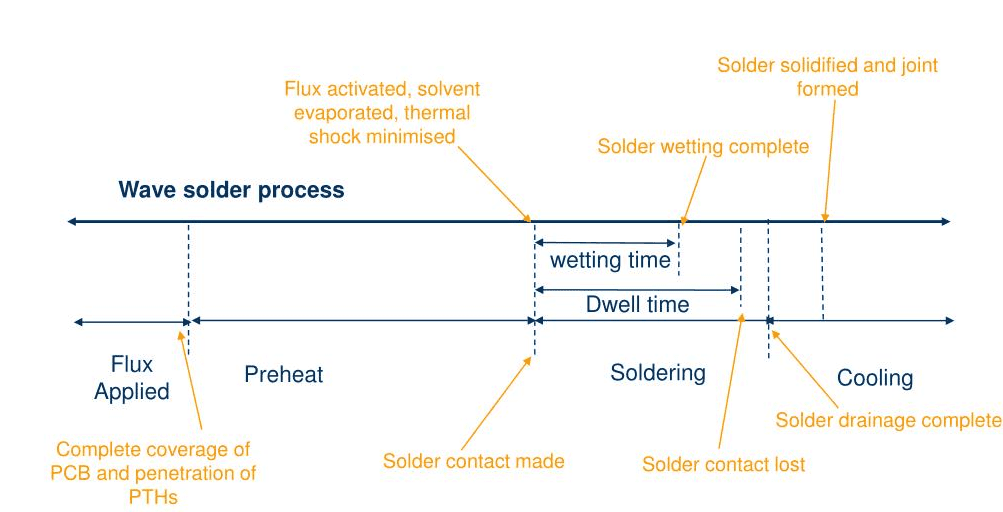
The Wave Soldering Gadget
When working with a wave soldering gadget, you should pass your printed circuit board over a unique wave of molten solder paste for you to solder electrical components to your PCB. Moreover, before the soldering process starts, in this case, you have to apply a flux layer onto the circuit board to effectively clean the pads and component contacts to make sure that the solder paste adheres properly.
After applying the flux layer, you then pre-heat the printed circuit board to prevent any thermal shock from occurring. Lastly, set up a solder wave within a special tank containing molten solder. Pass the circuit board over the wave such that the circuit board’s underside touches the solder wave generating an electrical connection between various contacts and lead components and their respective pads and holes.
However, you should note that this technique is not popular nowadays. That’s because the reflow soldering method is more effective and it has more advantages; hence manufacturers tend to go with it instead of the wave soldering method. As a result, technicians primarily utilize the wave soldering process to tackle the assembly of THT components.
Unique Advantages of the Wave Soldering Process
The wave soldering process also comes with a few advantages, which include:
Reduced Warpage
When utilizing the wave soldering process, the printed circuit board tends to spend less time in contact with the high temperatures that technicians use in the soldering process. Doing so can effectively reduce printed circuit board warpage making the PCB more efficient.
Improved Solder Joint Quality
The various sufficient activities that take place during the wave soldering process ensure that the solder joints that emerge from this process are of high quality compared to those that occur from reflow soldering.
Inspection
Auto Optical Inspection
After assembling all the necessary electrical components onto the circuit board, it’s time to inspect and test the PC board. However, since PCBs have become pretty complex over time, manufacturers must now work with complex auto-optical inspection gadgets to inspect their circuit boards more effectively.
While technicians can still utilize manual means, such as visually pointing out mistakes, this isn’t effective when they are dealing with mass production. That is because humans naturally get exhausted. After going through a couple of circuit boards, they get tired and start overlooking mistakes.
PCBA testing is a vital step in PCB assembly that technicians can’t afford to skip. It helps them avoid costly rework fees. Moreover, ignoring this phase can lead to wastage of PCB materials, which adds to list of losses you can avoid.
Manufacturers employ AOI systems to effectively detect ad report issues early in the PCB production process. Moreover, this system lets technicians modify individual processes and circuit boards for more efficient rectifications before things get out of hand.
By utilizing optical techniques to effectively detect and report defects, auto-optical inspection gadgets can undertake checks that humans previously carried out with more accuracy and speed.
Generally, the AOI gadget utilizes complex cameras to capture the board’s surface. It then generates an image that it utilizes to analyze the entire board. The gadget then compares the analysis image with the image of the reference board (the board containing all the specifications). By using this comparison, the AOI gadget is able to pinpoint various defects, which include:
- Scratches
- Shorts
- Missing components
- Incorrect components
Conclusion
PCB component assembly machines come in multiple variations depending on their applications in the PCB manufacturing process. For example, there are PCB component assembly machines for applying solder paste, applying special glue, soldering the components, and much more. All these machines are crucial to the PCB assembly process. Therefore, before diving into the world of PCB production, you have to grasp how each works. We hope that this article has answered all the questions that you had regarding PCB component assembly machines.
