Hosting an event is as simple as securing a venue and decorating it to standard. Make payments on various important needs in achieving a classic event, and the event is ready I guess? That could be the feelings until the unplanned such as an act of God (heavy rain) brings about setbacks.
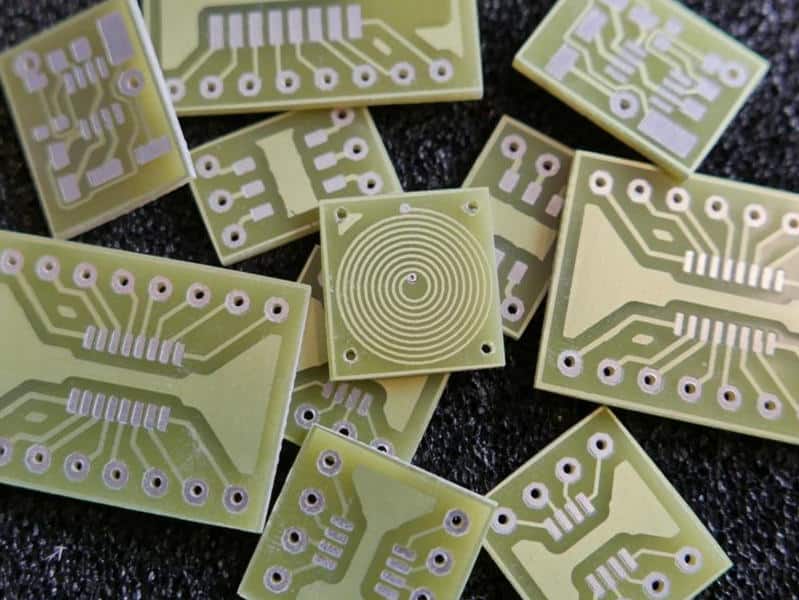
In reality, there are out of sight factors in planning and hosting a classic event. Such are little details that require adequate attention in designing a quality PCB. Producers could be a victim of an ineffectual PCB if attention is not given to little details.
During the PCB manufacturing process, various tasks are on concurrently. There could be an excessive or an insufficient use of materials on the design as a result. These shortcomings could cause a structural defect or integrity failure on the PCBs. Hence, the need to check through each stage of production and make corrections needed.
PCB Etching is such a little detail that is very essential to the PCB design. Etching is the careful deletion of materials for the exterior layer of the PCB. Chemical and etching agents help in the removal process.
Request PCB Manufacturing Cost, Pls Send PCB Files to Sales@raypcb.com NOW
Etching PCB
As the PCB industry evolves, the resistivity demands by different wires in use went up the scale. Stern management of such wire diameters becomes non-negotiable in PCB designs.
Also, PCB standards are advancing as much as its designs are experiencing diversification. Thus, the etching techniques in the PCB manufacturing process also gained popularity. The PCB etch strategy is to clean out the surface layers of conductive materials that are in excess. These strategies are in two broad categories, they are wet etching and dry etching.
Wet etching
This is the system whereby the copper layer gets plunged into the etching chemical fluid. Wet etching is the most popular method adopted for use. Some elements impact the rate of its performance. They are etching solvents ambient, solvent concentration and its gripping. It also does not change properties in all directions.
There are two procedures through which wet etching is commonly used. Each of the mediums has their benefits and setbacks.
Soluble/Alkaline etching process
This etching procedure is often used to carve out the surface layer in a PCB using solvents. It is a speedy exercise but costly. This process requires that the chemical specification for use is adequately observed.
Its implication being that the board could get damaged if left for a lengthy period of time. Furthermore, there are other specifications that are necessary for consideration during this process.
They are the solvent spritz, rate of layer movement and the quantity of excessive copper on board. Putting them in perspective would guarantee an equitable etching process with leveled baseboards.
Note, there is a breakpoint in the course of this etching process. It is when the carving out of the excess copper is completed. Some of the solvent used are hydrogen peroxide, hydrochloride, Chloride copper and water.
Acidic Etching Process
Unlike the alkaline etching process, this procedure has its focus on the inner layers of a rigid PCB. It is cost effective and direct but wastes time. Its execution is for inner layers. This is due to the fact acid does not respond to photolithography neither will it destroy the needed part.
Also, the edgeways waste materials below the copper tin/surface layer are small. The lines covered on the PCB are safe while the solvent attacks the copper. The lines are safe as a result of the coverage given to them by photo resist or a plated etch resistant. Chemicals used for this process are Cupric Chloride or Ferric chloride
Dry etching
The dry etching procedure is also known as plasma etching. This process adopts the usage of machines to etch out coppers with no left over residues. Its operation is less stressful compared to the wet etching process. It is a perfect choice for large volumes of PCB production.
Furthermore, the process is less demanding in dealing with residue disposal. The excess copper is always released to the airspace making the process a cleaner way to etch.
PCB Etching Process
PCB etching serves as one significant step in the concluding process of PCB design. It means the taking out of the inordinate copper to unveil the correct pattern of the design.
Printing a PCB on a flat metal piece to unveil line design is a complex process of visual and chemical charge. At present, the means to process a PCB is through model plating. This implies adding a lead tin resistant to the surface layer in a bid to preserve the copper foil on the board. And as such, the leftover copper is chemically removed.
In PCB etching, there are two sides of patterned layers of copper on the board. Nonetheless, a layer of copper in the outer surface of the board must be totally removed. The leftover copper makes up the needed circuit for final design. This etching process is a model described only on the PCB with a lead tin resistant layer.
Furthermore, full copper plating procedure is the other method for PCB etching. It involves covering the whole board with copper except for the lead tin resistant part. The copper coverage is done two times round the board during this process. However, copper must be taken out of the board while etching.
This process is notable for its huge disadvantage that comes with removal of the copper. Corrosion is an after effect that could change the conformity of lines as well as shift in wire width.
Likewise, removal of metal plated layer to a light reactive layer is also a PCB etching process. It is close to the etching process used for inner layers. Lead tin is used as the resistant layer in the etching process.
PCB Etching Solution
PCB etching solution is a poisonous waste. They produce harmful vapors, cause blemish and eat up metallic components. Essential to the PCB manufacturing process, therefore it is vital to grasp its safe usage.
There are various etching solutions convenient for use. They include cupric chloride, sodium persulphate, ferric chloride, ammonium persulphate among others.
Ammonium Persulphate Solution
This type of chemical solution is adaptable to tin resistant processes. It allows for visibility while working, less combative and it needs high temperature. Also, vapors emitted are poisonous. Ammonium persulphate decays into base metal sulfur and nitrogen that aids ignition.
Ferric Chloride Solution
Unlike the ammonium persulphate, it is an etching solution that is combative. It is cost friendly and serves as solvent used for waste treatment to isolate hard waste. Furthermore, it has a rusty color which hides the etched material. It blots whatever component it has contact with.
Sodium Persulfate
This is an etching solution with an average water and acidic soluble. It is a plain chemical that allows a clear view of its working process. It has a great adaptable strength with the resist pen and it is an expensive choice for etching. However, it is a toxic waste due to its combustive nature.
Cupric Chloride
This etching solution is an inanimate copper chloride made from etching copper mixture. It appears as a yellowish dust, non-combustible, acidic to aluminum and could become a danger. It is a solvent that generates hydrogen chloride gas if heated in fire. Also, it allows addition of hydrogen peroxide when depleted.
Request PCB Manufacturing Cost, Pls Send PCB Files to Sales@raypcb.com NOW
DIY PCB Etching
DIY PCB etching implies manufacturing the PCB yourself or etching pcb at home. It involves following each step and all the required elements to fabricating a PCB.This production process also entails etching the PCB. You can etch the PCB individually at home or the laboratory.
Design the PCB
The next appropriate step is to design the PCB through the Eagle platform. At the completion of the design, two files consisting of the schematic and board come up. Mark the layer option and unmark others that are not necessary. Transport the board file in image form and then click on the color film before saving the image.
Print PCB
The printing process of the designed PCB comes up next. The printing of the image is done on a see-through plastic sheet. The laser printer is the best suitable option for this type of printing.
The settings on the laser printer must read high resolution printing and not high speed. This is to enable a full and proper transfer of the image on the board. It is also vital to open the image and select the invert color box before the image is finally saved and printed.
Toner Transfer
Toner transfer involves placement of the printed image on the copper board. The circuit page lays cladding down, covered with a cotton cloth in readiness for heat using an iron.
The iron rests on the cloth in a vertical position barring any movement sideways for two minutes. After the stipulated two minutes, the iron can then move with force asserted. The movement has to be gradual to avoid blotting the print. The board needs a cool off period of five minutes before taking out the plastic sheet from an edge. It is vital to apply force during the ironing for firmness.
Etching
This process deals with solvents that are acidic and so proper safety measures are vital. Ferric chloride (powdered) etching solution is the perfect choice for this task. It requires liquefying the solvent in warm water, blended until it disintegrates.
Choose a malleable bucket that could house the copper board and shake the mixture with a rod. It is important to note that the full board should not go into the etching solution at once. The copper at the edges first before it removes the copper at the centre.
The etching process takes approximately 15 minutes. Take out the board with a plier to avoid physical contact with the hand and rinse under running water. Put it out to get dried and apply acetone to get rid of the toner prints from the board.
Safety requirements for this process include: safety goggles, hand gloves and nose mask. To avoid contacts with the eyes, skin and to avoid inhaling the toxic acid. During this etching process, add Ferric chloride to water and not water to it.
Solder Mask Application
To prevent the copper from corroding and adding an extra shield to the layer, the need for a solder mask. Before this step, it is necessary to change the layer setup on the eagle platform such that pads only are seeable.
Transport it in image form and print on a translucent paper. Apply a tiny film with an ultra violet reactive solder and position the dark pads with the sheet on the board. Attach with a paper clip while it is under the sun for 15minutes to allow the solder mask steeled.
Drilling
Drilling the holes to allow fixing electronic elements is next. The PCB drilling machine and the drill bits that match the diameter of the pins are the needed tools. While drilling, the board should be properly placed on a wooden platform. This is to allow the drill bit probe through the board easily.
Soldering
Soldering enables the elements required on the board to be well fixed. Solder iron aids the fixing process with flux to solder the pins to the board.
Testing
This is to check the correctness of all connections on the board. A multi tester put in continuity mode will perform the checks. To achieve this, one pin of the multi tester pins touches a joint and the other touches the tail end of the copper trace. If the connections are perfect, there would be a bell sound.
Laser PCB Etching
The PCB laser etching is a process whereby high voltage laser machines shape out trace lines on a PCB layer. It is a process used to reduce the number of vigorous steps in the manufacturing process. It also helps to get rid of using toxic etching solvents, inks and acids.
The PCB laser machine aids the removal of materials not required on the PCB through etching. It could come as simple as spritzing the selected area for removal and the PCB laser machines do the rest.
Its invention came up to help the etching process. This is by disintegrating the PCB in a most effective and efficient way. PCB etching done manually requires the use of hydrogen chloride and water. Afterwards, the PCB gets dipped into the tray that contains the etching solution.
This process is accident prone such as spillage, contacts with the skin and all kinds. It is also time consuming and could also cause damages to the PCB in some instances.
It is on this premise that the invention of PVC solvent that could melt copper became a necessity. The PCB etching machine moves the etching solution through air to hasten up PCB etching. The machine functions as dependent on the size of the PCB. It also enchants the etching solutions that are threatening if inhaled.
Conclusion
As important as the etching process is to the PCB manufacturing process, it could be very tasking. Having the technical know-how of how it works will help achieve the set target.
