A PCB kit contains the materials you need to build a board. The materials are often available at local hardware stores or electrical stores. In some cases, you can get bulk discounts from these stores. Other times, you can purchase a PCB kit online. Just make sure you look for reviews and choose a reputable online retailer.
A PCB kit includes single-sided, double-sided, or multilayered one. Flexible PCBs are much thinner and lighter than rigid PCBs. They also can be shaped to fit small spaces. Because we shape them to fit a particular space, they tend to be more affordable than rigid ones.
Printed Circuit Board Materials
We construct double-sided printed circuit boards from a variety of materials. For example, one type consists of foil bonded to an insulating base material. The insulating base also contains electrical materials mounted on the kit on both sides. We achieve the interconnections between conductive patterns through plated through holes.
The materials helpful in printed circuit boards are classified based on their electrical properties. The FR4 material is commonly essential for standard applications, but various other materials are available. For example, a high-Tg version of FR4 is also available for improved thermo-mechanical properties. High-frequency applications, on the other hand, require alternate materials.
PCB Materials include polyimide, phenolic, polyester, and Mylar. These materials help make flexible printed circuit boards for aerospace and medical devices. They are also ideal for the construction of heavy-duty equipment. In addition, some of these materials are fire-resistance, and we can use them in various temperature conditions.
Etching process and PCB making supplies
Using kitchen supplies to etch a circuit board can be very easy. This project requires a little bit of preparation. You’ll need a kit that’s the correct size and a hacksaw to cut it to size. You can also use a hand or electronic driller to drill holes for mounting materials. However, if you’re using SMD components, you may not need to use a driller at all.
Alkaline etching
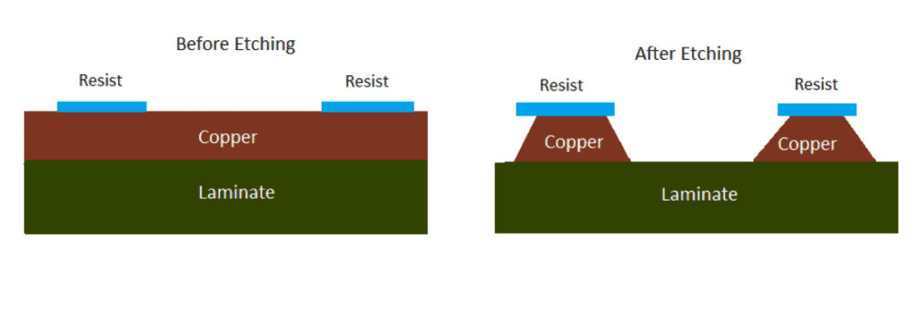
Alkaline etching on a kit is easy to perform at home with a few common kitchen supplies. It’s helpful to remove unwanted kit from circuit boards. The chemical solution is a brown liquid usually sold in concentrated form. First, soak the PCB in the solution and keep an eye on it periodically. Although heating the solution will speed up the process, it isn’t necessary. Alternatively, you can use a clear liquid called ammonium persulfate.
The acidic etching solution will not react with the photoresist on the board, and it takes longer than the alkaline one. It also produces a less severe undercut in the copper, a desirable trait. However, it is essential to watch the temperature of the solution to avoid damaging the kit.
Acidic etching
Before you start, it’s essential to understand how acidic etching works. This process will remove the foil, leaving a thin layer of tin underneath. This tin acts as a protective layer for the copper. As a result, the copper circuitry below will no longer be intact, leaving an acid trap on the circuit board.
Acidic etching a circuit board is similar to chiseling rocks, but it requires a lot more patience. Removing the copper traces on the kit won’t take long. Then, you’ll need to ensure you have the board’s proper layout design.
Cleaning the copper surface
You can clean a circuit board’s surface using household supplies. You can mix baking soda and water to create a paste. After applying the paste to the kit, brush it with a clean, soft brush. Then let it dry. After it dries, use distilled water to rinse the kit. Next, use a household cleaner to remove the remaining corrosion. Lastly, wipe the kit dry with a lint-free cloth or microfiber towel.
To clean the copper surface of a circuit board, you can use non-phosphate detergents. You can also try using rubbing alcohol. However, it will be a bit more expensive. In addition, this solution is not as effective as other cleaners. After cleaning the kit, it’s essential to let it dry thoroughly before replacing the attach components.
PCB Layout And Design Software
There are a variety of PCB layout and design software options available today. However, if you’re looking for an easy way to design circuit boards, you should check out DipTrace. This software can design and manufacture circuit boards and supports Altium, Eagle, PADS, and various 2D/3D CADs. It also offers manual routing, high-speed signals, and Gerber and STEP export. The software also includes several helpful editing tools.
Cadence
Cadence PCB layout and design software is a flexible solution that allows designers to create complex circuit boards easily. It provides an environment that supports constraint-driven flow, enables concurrent workflow updates, and offers extensive features. It also addresses challenges related to PCB manufacturing, including power integrity, interconnects optimization, and signal integrity. In addition, it supports all stages of the design process and has an integrated constraint management system.
The software comes with a range of useful tools, including schematic capture. A schematic is a 2D electrical design that illustrates connections between electronic devices. It costs from $2,800 to $3,000 for a license for the Allegro version. For more advanced designs, users can also opt for the more expensive OrCAD PCB Designer Standard or Pro versions, which range from $2,300 to $7,140.
Altium
The Altium PCB Layout and Design software has advanced 3D layout tools and a unified set of design tools. This software makes multi-board design a breeze. Its native 3D MCAD engine lets you view your circuit board panels in 3D during panelization. It also helps you prepare your design for PCB fabrication.
Altium PCB Layout And Design Software is a high-end EDA software. Although its price is somewhat steep, it has a free trial version and an affordable perpetual license. It also offers a cloud storage service and unlimited training. However, the software does have some disadvantages.
Altium Designer offers a suite of advanced routing features that simplify the creation of complex circuit boards. It includes automatic trace widths routing and impedance control. It also has inbuilt topological auto-routing.
Cadence Allegro
Allegro PCB design software is a full-featured design suite that supports the entire PCB design process. Its scalable design environment is ideal for both small and large companies. It supports a broad range of file formats and supports the import/export of design data from other EDA suppliers. In addition, the software’s comprehensive feature set includes advanced simulation and debugging capabilities.
Cadence offers several PCB layouts and design software tools. The main one is the Allegro PCB Designer. This software is a bit more complex than other alternatives, but it allows users to break down their design tasks into several applications. Additionally, this software is usually more memory-efficient due to its ability to break down its functions.
ZenitPCB Layout
ZenitPCB Layout And Design Software is a Windows-compatible PCB design suite that enables you to create complex circuits with up to 1000 pins. It has various tools that allow you to create a design quickly and easily, from schematic capture to a finished layout. In addition, the software has built-in tools that can read Gerber files and let you make adjustments.
Aside from its powerful circuit design tools, ZenitPCB also features a library of through-hole materials, auto-routing, and netlist import. It’s also free and comes with a comprehensive environment. It’s easy to use and intuitive. More than 40,000 engineers use it.
KiCAD
KiCAD is an open-source PCB layout and design software suite that is free to use and runs on Mac, Windows, and Linux. It offers an extensive library of materials and symbols and supports the creation of complex circuit diagrams. In addition, it exports Gerber files and supports photo-plotting, drilling, and component location.
To create a new project, you must first create a schematic. Next, you must choose the kit layout. To do this, open the Schematic Layout Editor (also known as Eeschema) and double-click the schematic file. Alternatively, you can click on the ‘New Project’ button.
KiCad’s schematic editor is easy to use and has many valuable features. It supports multiple languages, hierarchical schematic sheets, and custom symbols. The software also features integrated ngspice circuit simulation. It also has a 3D viewer that lets you view your PCB fully and preview it before printing it. Its built-in raytracer and adjustable lighting can help you create complex circuit boards faster.

Advantages and Disadvantages of Hybrid printed circuit boards
Hybrid PCBs are a combination of two types of printed circuit boards. One type consists of a rigid printed circuit board and the other consists of a flexible substrate. A flexible substrate enables the PCB to be folded and placed on irregular surfaces. Another type features an additive printing process that generates less material waste. Despite the advantages of hybrid PCBs, they have not yet reached the market. Therefore, further testing is necessary before adopting them into practice.
In addition to their versatility, hybrid PCBs are inexpensive, which makes them an excellent option for many electronic applications. However, they can lead to lower-quality circuit boards that do not fulfill the desired functions. Hybrid PCBs can be made from cheaper materials when the application does not require high frequencies and functions and more expensive materials when the PCB has higher electrical and mechanical properties.
Hybrid PCBs are also useful in hot-pluggable customer applications. For example, one kind of hybrid PCB may operate at speeds up to 25 gigabits per second. In addition, it may contain super-fine connecting elements of up to 50 microns, allowing it to transmit information at high speed.
Hybrid PCBs consist of copper and other materials that interact with one another. However, they are vulnerable to layer separation. During temperature changes, different materials will expand or shrink and cause the layers to separate. When this happens, copper interfaces on the substrate can peel off and peel away from the laminate layer. Therefore, it is essential to be aware of the exact time when delamination will occur.
How to Make Your PCB Kit – The Process
There are several ways to design a PCB. For example, you can use a small surface-mounted component with a low profile, allowing you to make a smaller PCB. Alternatively, you can use a through-hole component, which is larger but easier to find and solder.
Designing a PCB
Before designing the PCB layout, you should determine your PCB’s purpose. You can do this by considering the components you’ll be placing and how they connect to other circuits. You’ll also need to consider the materials helpful and the operating environment where you will place your PCB. These are all critical decisions in the design process. Also consider body and eye protection when working.
Choosing your components is another important step in the process. Choose components that fit your product specifications and those that are compatible with your assembly process. Consider the size of component packages and noise and shielding requirements. You’ll also need to know the spacing and the components’ trace widths.
Prepare the PCB Kit Transfer Paper
The first step in preparing the PCB kit Transfer Paper is cutting your copper board to size. You can do this using a cutter or hacksaw. Once you cut the kit, use abrasive sponge scrubs or steel wool to remove top oxide layer and photoresist layer. This will make it easier for the image from the paper to adhere to the kit.
Then, print the image onto the paper at the right scale and resolution. Select the highest density setting and print the image on the light blue side. Cut out several copies of the design, if necessary. You can also tile the designs onto one sheet. You must make sure to leave minimal margins for alignment.
Adding a laminating press
A laminating press is a useful tool for making PCBs. It fuses double-sided PCB layers by applying pressure and heat to a stack of PCBs. The press can fuse up to five layers simultaneously. We do the laminating process using specialized pins.
We place the PCB stack-up under high pressures and temperatures for about two hours. After completing the press cycle, we unmold and prepare the PCB for registration holes. It is then deburred and rounded at the corners. The process starts with the substrate and laminate, which are the building blocks of a circuit board. These can be custom-designed to meet the needs of a particular device.
Adding a photoresist layer
Adding a photoresist layer is an essential part of the PCB design process. However, it requires careful preparation before starting. First, we print your PCB design onto a laminate panel. The laminate is then pre-bonded with copper. After that, you must etch the copper to reveal the PCB blueprint. Then, you apply a photo-sensitive layer called photoresist. This photo-sensitive layer consists of chemicals that harden when exposed to UV light and ferric chloride. This will allow the technicians to match the image with the blueprints.
After the photoresist is exposed, you need to remove it chemically. This will allow you to see the copper underneath. After that, you will need to etch the copper again. In this step, you need to use a fine metal-cutting blade with plenty of tension. Also, you need to place thin cardboard on both sides of the PCB to protect the photoresist. After this, you can clamp the PCB with a piece of wood or cardboard to prevent scratches.
Next, you need to prepare your double-sided PCB for UV exposure. The exposure time depends on the strength of the UV light. Typically, it takes about five minutes to cover one side of the PCB photoresist. After that, you should prepare a developer solution. This will dissolve the unwanted photoresist parts while leaving the traces intact.
Adding a silkscreen layer
Adding a silk screen layer to your computer-basic board (PCB) kit is an easy and inexpensive way to add a unique design to your board. It can add color, text, or other information to your PCB. We print the silk screen over the PCB’s solder mask. Therefore, the silkscreen must be readable and match the color of the PCB solder mask. It should also follow CM’s dimensions and clearance guidelines to avoid being covered by other components.
Silkscreens are made from non-conductive epoxy ink and are available in many colors. We often print silk screens to include text-based information, such as parts or circuit points. Some silk screens include warning signs, such as high voltage or grounding. They can also be helpful for beautification purposes. However, they must be legible and not distracting.
Print Your Transfer Design on a PCB using a laser printer
If you’re using an inkjet printer, transferring the design onto the PCB can be difficult because the toner doesn’t stick to the copper very well. You can improve your transfer quality by sending the paper through your laser printer twice. This will eliminate the problem of a thin line or dot on the warm drum.
Before you start your transfer process, you must clean your copper board. Use an acetone-based scrub to remove dirt and grease from the copper surface. Dirty copper will not allow the toner to adhere. You should scrub every square millimeter of copper and regularly switch to a new towel. You should also cut out your design, leaving a minimal margin around the edges. By doing this, you’ll make the alignment process easy. Ensure there is adequate eye protection when dealing with the laser printer.
Apply PCB Toner Transfer Paper
A PCB toner transfer paper is a must-have if you want to make printed circuit boards. Generally, this type of paper uses a silicone release backing that helps release toner with minimum force. Silicone release backings are available for various printers, including the Avery laser printer. If you don’t want to purchase silicone release backings, you can make your silicone release paper by cutting a sheet from regular printer paper. Or you can use a silicone windshield sealer. Then, if you want a very clean surface, use a stiff squeegee to press the silicone into the paper fibers using a laser printer.
Toner transfer paper is a versatile and inexpensive craft material that makes transferring toner onto a surface as simple as paper. With a simple Xerox copy machine, a foam brush, and some matte medium, you can create a transfer without breaking the bank. Toner is often available at any copy store, and you can use toner printouts to create a transfer at home.
White toner printers are only as good as their toner transfer paper. To ensure the best results, use high-quality white toner transfer paper. The right paper will help your printer perform as efficiently as possible, and it will also help you avoid wasteful and messy liquid ink. For this reason, we recommend purchasing polymer-coated transfer paper to use on a variety of materials.
Toner transfer paper is an excellent choice for prototyping purposes, and its fast turnaround time makes it an excellent choice. However, it’s important to remember that toner transfer paper isn’t perfect on the first try. To avoid any issues, we recommend using a professional heat press when applying your transfer paper.
Adding components
To add a component to a PCB kit, you must have a footprint of that component. You can create these footprints in the PCB Library Editor, and we will place these footprints automatically when you transfer your design from the schematic editor to the PCB editor. The PCB Library Editor uses Design Synchronization to detect the differences between the schematic and the PCB and will automatically place the component.
After determining the area needed for the placement of devices, you should place the pads and interior parts. You should ensure that the parts do not overlap and that there is enough space between them. If you do not place them carefully, you may have to redo the whole board.
The next step is to design the double-sided PCB. The PCB Editor has a Defaults page where you can specify the properties of each component. You can manually set these properties if you don’t want to use the Defaults page. If you make changes to the defaults, these settings will apply to all subsequent Components you place on the PCB.
