PCB layout and design is an essential part of the electronics manufacturing process. It involves creating a physical layout of the printed circuit board (PCB) that connects different electronic components to each other. The design of the PCB plays a vital role in the overall performance and functionality of the electronic device.
Designing a PCB layout requires expertise and knowledge of various factors such as the number of components, the size of the board, and the type of circuitry. A well-designed PCB can reduce the risk of errors, improve functionality, and lower the cost of production. With the increasing complexity of electronic devices, the demand for high-quality PCB layout and design services has also increased.
Professional PCB layout and design services can help ensure that the PCB is designed to meet the specific requirements of the device. These services can also provide assistance with the selection of components, routing, and optimization of the layout. By outsourcing PCB layout and design services, companies can save time and resources while ensuring that the final product meets the highest standards of quality and performance.
PCB Layout and Design Services
Overview
PCB layout and design services are essential for any company that wants to manufacture electronic products. These services provide a complete solution for designing and manufacturing printed circuit boards (PCBs) that meet the specific requirements of the product. PCB layout and design services include schematic capture, component placement, routing, and verification of the design.
Benefits
There are many benefits of using PCB layout and design services. First, these services provide a complete solution for designing and manufacturing PCBs, which saves time and money. Second, PCB layout and design services ensure that the design is optimized for performance, reliability, and manufacturability. Third, these services use advanced software tools and techniques to ensure that the design meets all the necessary standards and regulations.
Process
The PCB layout and design process typically involves the following steps:
- Schematic capture: This involves creating a schematic diagram of the circuit design.
- Component placement: This involves placing the components on the PCB in the most optimal way.
- Routing: This involves creating the traces that connect the components on the PCB.
- Verification: This involves checking the design for errors, such as short circuits or incorrect component values.
PCB layout and design services may also include additional steps, such as thermal analysis, signal integrity analysis, and design for manufacturability (DFM) analysis.
In conclusion, PCB layout and design services provide a complete solution for designing and manufacturing PCBs that meet the specific requirements of the product. These services offer many benefits, such as saving time and money, optimizing the design for performance and reliability, and ensuring that the design meets all the necessary standards and regulations.
PCB Layout Services

Our PCB layout and design services provide a comprehensive solution for your printed circuit board needs. Our team of experienced engineers and designers are dedicated to delivering high-quality PCB layouts that meet your specific requirements.
Single Layer PCB Layout
Single layer PCBs are the simplest and most cost-effective option for low complexity circuits. Our single layer PCB layout services ensure that your design is optimized for manufacturing, minimizing the risk of errors and reducing lead times. We use industry-standard software and design practices to ensure that your PCB is reliable and meets your specifications.
Double Layer PCB Layout
Double layer PCBs are suitable for more complex circuits that require additional routing options. Our double layer PCB layout services ensure that your design is optimized for signal integrity and manufacturability. We use advanced design techniques to minimize noise and interference, ensuring that your PCB performs reliably.
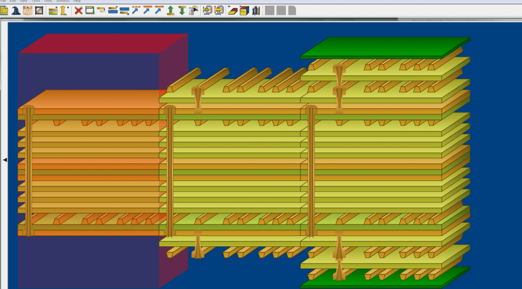
Multi-Layer PCB Layout
Multi-layer PCBs are suitable for high complexity circuits that require multiple layers of routing. Our multi-layer PCB layout services
PCB Design Services
Our PCB design services offer comprehensive solutions for all your printed circuit board needs. We specialize in designing custom PCBs for various applications, ranging from simple to complex designs. Our team of experienced engineers has the expertise to deliver high-quality PCBs that meet your specific requirements.
Schematic Capture
Our schematic capture services involve creating a detailed diagram of your PCB design, including all the electrical connections and components. We use industry-standard tools to create accurate schematics that are easy to understand and modify. Our team works closely with you to ensure that the schematic captures all the necessary details of your design.
Component Placement
Our component placement services involve placing all the components on the PCB in the most optimal manner. We take into consideration factors such as signal integrity, thermal management, and manufacturability when placing the components. We use advanced software tools to ensure that the components are placed in the most efficient manner possible.
Routing
Our routing services involve creating the physical connections between the components on the PCB. We use advanced routing techniques to ensure that the PCB has the best possible signal integrity and thermal management. We also take into consideration any specific requirements you may have for the routing, such as high-speed or high-power signals.
In conclusion, our PCB design services offer a comprehensive solution for all your printed circuit board needs. We have the expertise and experience to deliver high-quality PCBs that meet your specific requirements. Contact us today to learn more about our services and how we can help you with your next PCB design project.
Quality Control
Design Rule Check
Design Rule Check (DRC) is a crucial step in PCB layout and design services. It ensures that the design meets the industry standards and specifications. The DRC process includes checking the PCB layout for issues like clearance errors, trace width errors, and spacing errors. The DRC process is done using specialized software that checks the design against a set of rules and generates a report of the errors found. The report is then reviewed by the design team, and the necessary changes are made.
Signal Integrity Check
Signal Integrity Check (SI) is another essential step in PCB layout and design services. It ensures that the signals transmitted through the PCB are not distorted or degraded. The SI process includes analyzing the PCB layout for issues like crosstalk, reflections, and signal loss. The SI process is done using specialized software that simulates the signal behavior and generates a report of the issues found. The report is then reviewed by the design team, and the necessary changes are made.
Electrical Testing
Electrical Testing is the final step in PCB layout and design services. It ensures that the PCB meets the functional requirements. The electrical testing process includes testing the PCB for issues like open circuits, short circuits, and impedance issues. The electrical testing is done using specialized equipment that tests the PCB for the specified parameters. The test results are then reviewed by the design team, and the necessary changes are made.
In conclusion, Quality Control is a critical aspect of PCB layout and design services. The DRC, SI, and Electrical Testing processes ensure that the PCB meets the industry standards and specifications, and the functional requirements are met.
Turnaround Time
When it comes to PCB layout and design services, one of the most important factors to consider is turnaround time. This refers to the amount of time it takes for the service provider to complete the design and deliver the final product to the customer.
The turnaround time can vary depending on the complexity of the design, the number of layers, and the size of the board. However, most professional PCB layout and design services offer a standard turnaround time of 2-3 weeks for a typical 2-4 layer board.
For rush orders or more complex designs, the turnaround time may be longer and will typically come with an additional fee. It’s important to discuss your project timeline and requirements with the service provider before placing an order to ensure that they can meet your needs.
Some PCB layout and design services offer expedited turnaround times for an additional fee. This can be a great option for those who need their boards quickly or have a tight deadline.
It’s important to keep in mind that while a shorter turnaround time may be desirable, it’s also important to ensure that the quality of the design is not compromised. Rushing a design can lead to errors and mistakes, which can result in costly delays and revisions.
In conclusion, when choosing a PCB layout and design service, it’s important to consider the turnaround time and ensure that it aligns with your project timeline and requirements. A reliable and experienced service provider will be able to provide a realistic estimate and deliver high-quality designs within the agreed-upon timeframe.
Pricing
When it comes to PCB layout and design services, pricing can vary depending on a number of factors. Some companies charge a flat rate for their services, while others charge by the hour. Additionally, the complexity of the project can also impact the final price.
It’s important to do your research and compare prices from different companies to ensure you’re getting a fair deal. Keep in mind that the cheapest option may not always be the best option, as quality and experience can also play a role in the final product.
Some companies may also offer additional services such as prototyping, testing, and assembly, which can add to the overall cost. Be sure to clarify exactly what services are included in the price quote to avoid any surprises down the line.
Overall, while pricing is an important factor to consider when choosing a PCB layout and design service, it’s not the only factor. Quality, experience, and additional services should also be taken into account to ensure a successful project.
Conclusion
In conclusion, PCB layout and design services are a crucial aspect of any electronic product development process. They ensure that the final product is reliable, cost-effective, and efficient.
By outsourcing PCB design services, you can benefit from the expertise of experienced professionals who have a thorough understanding of the latest industry standards and technologies. This can save you time, money, and resources while ensuring that your product meets all the necessary requirements.
When choosing a PCB design service provider, it is essential to consider factors such as experience, expertise, and reputation. Look for a provider who has a proven track record of delivering high-quality services on time and within budget.
In summary, outsourcing PCB layout and design services can help you streamline your product development process and ensure that your final product meets all the necessary requirements. By partnering with a reliable and experienced provider, you can achieve your product development goals while minimizing risks and optimizing costs.
