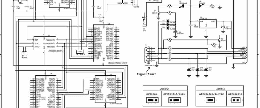
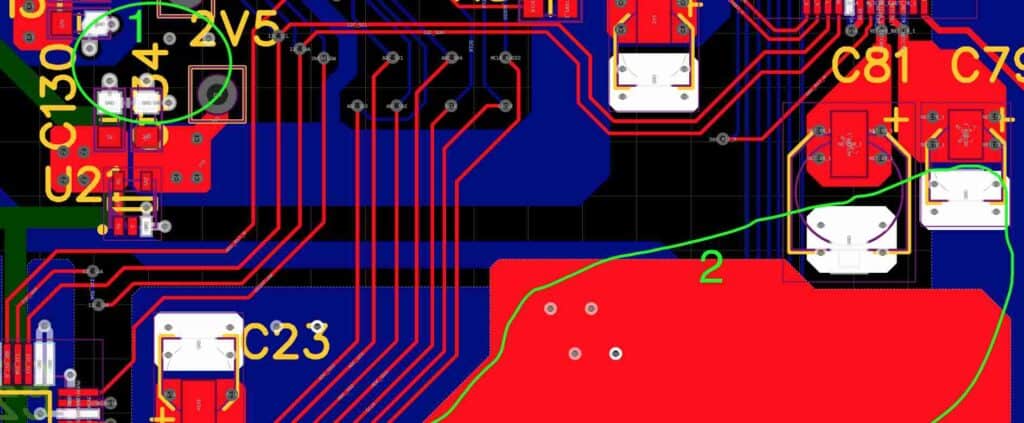
PCB layout to schematic converter is a tool that facilitates the design of printed circuit boards (PCBs). It is a software application that allows users to convert the layout of a PCB into a schematic diagram. This tool is particularly useful for engineers and designers who work on complex PCB designs.
The process of designing a PCB involves creating a schematic diagram of the circuit, followed by laying out the components on a PCB. The schematic diagram provides a visual representation of the circuit, while the PCB layout determines the physical arrangement of the components. The PCB layout to schematic converter simplifies this process by allowing users to create a PCB layout and then automatically generating a schematic diagram based on that layout. This tool can save time and reduce errors in the design process.
PCB layout to schematic converter is an essential tool for PCB designers and engineers. It streamlines the design process and helps to ensure that the final product is accurate and reliable. With this tool, designers can easily convert their PCB layouts into schematic diagrams, saving time and reducing errors in the design process.

What is a PCB Layout to Schematic Converter?
A PCB layout to schematic converter is a software tool used to convert a printed circuit board (PCB) layout into a schematic diagram. This tool is commonly used by engineers, designers, and technicians who want to create a schematic diagram of an existing PCB layout or vice versa.
The process of creating a PCB layout can be time-consuming and error-prone. A schematic diagram, on the other hand, is a graphical representation of a circuit that makes it easier to understand and analyze. By using a PCB layout to schematic converter, you can save time and reduce errors by automatically generating a schematic diagram from an existing PCB layout or vice versa.
The PCB layout to schematic converter works by analyzing the PCB layout and identifying the components used, their connections, and their placement on the board. The converter then generates a schematic diagram that accurately represents the circuit, including component values, connections, and placement.
Overall, a PCB layout to schematic converter is a useful tool for anyone involved in the design or analysis of electronic circuits. It can save time, reduce errors, and make it easier to understand and analyze complex circuits.
Why Use a PCB Layout to Schematic Converter?
When designing a printed circuit board (PCB), it is essential to have an accurate schematic that reflects the desired circuit functionality. However, creating a schematic manually can be a time-consuming and error-prone process. This is where a PCB layout to schematic converter can be a valuable tool.
Here are some reasons why you might consider using a PCB layout to schematic converter:
-
Time-saving: Manually creating a schematic can take a lot of time, especially for complex designs. A PCB layout to schematic converter can save you time by automatically generating a schematic from the layout. This can be especially useful when you need to update a design quickly.
-
Accuracy: Manually creating a schematic can be prone to errors, which can lead to costly mistakes. A PCB layout to schematic converter can help ensure accuracy by automatically generating a schematic that matches the layout. This can help you avoid errors and ensure that your design works as intended.
-
Ease of use: A PCB layout to schematic converter can be easy to use, even for those who are not familiar with schematic design. This can be especially helpful for small businesses or hobbyists who may not have access to a dedicated schematic designer.
-
Cost-effective: Hiring a dedicated schematic designer can be expensive, especially for small businesses or hobbyists. A PCB layout to schematic converter can be a cost-effective alternative that can help you save money while still achieving accurate and reliable designs.
In summary, a PCB layout to schematic converter can be a valuable tool for anyone involved in PCB design. It can save you time, ensure accuracy, be easy to use, and be cost-effective.
Benefits of Using a PCB Layout to Schematic Converter

Using a PCB layout to schematic converter can offer several benefits to designers and engineers. Here are some of the advantages of using this tool:
1. Saves Time and Effort
Manually converting a PCB layout to a schematic can be a time-consuming and tedious task, especially for complex designs. Using a PCB layout to schematic converter can significantly reduce the time and effort required for this task. The software can quickly and accurately convert the layout into a schematic, saving designers and engineers valuable time.
2. Reduces Errors
Manual conversion of a PCB layout to a schematic can be prone to errors, and even small mistakes can have significant consequences in the final product. A PCB layout to schematic converter can reduce the risk of errors by automatically converting the layout into a schematic with high accuracy. This can help designers and engineers to avoid costly mistakes and ensure the quality of the final product.
3. Increases Efficiency
Using a PCB layout to schematic converter can increase the efficiency of the design process. With the software’s ability to quickly and accurately convert a layout into a schematic, designers and engineers can focus on other aspects of the design, such as optimizing the circuit, selecting components, and testing the design.
4. Provides Visualization
A PCB layout to schematic converter can provide a visual representation of the design, making it easier for designers and engineers to understand and modify the circuit. The software can generate a schematic with labels, symbols, and connections that can be easily interpreted, making it easier to identify potential issues or areas for improvement.
In conclusion, using a PCB layout to schematic converter can offer several benefits to designers and engineers, including time and effort savings, error reduction, increased efficiency, and improved visualization.
How to Choose a PCB Layout to Schematic Converter
Choosing the right PCB layout to schematic converter can be a daunting task, especially if you are new to the field. Here are some key factors to consider when making your decision:
Compatibility
First and foremost, you need to ensure that the converter you choose is compatible with both your PCB layout software and your schematic capture software. Some converters only work with specific software packages, while others are more versatile. Check the specifications carefully before making your purchase.
Accuracy
The accuracy of the conversion is crucial, as any errors in the schematic can lead to serious problems down the line. Look for a converter that is known for producing accurate results, and check user reviews to see if there are any common issues or complaints.
Ease of Use
A good converter should be easy to use, even for those who are new to the field. Look for a converter that has a user-friendly interface and clear instructions. Some converters even offer tutorials or online support to help you get started.
Features
Different converters offer different features, so it’s important to consider what you need before making your purchase. Some converters offer automatic netlist generation, while others allow you to customize the conversion process. Look for a converter that offers the features you need, without unnecessary extras that will only add to the cost.
Price
Finally, consider the price of the converter. While you don’t want to skimp on quality, you also don’t want to overspend. Look for a converter that offers good value for money, and compare prices between different brands and models to find the best deal.
By considering these key factors, you can choose a PCB layout to schematic converter that meets your needs and helps you to create accurate, error-free schematics for your PCB designs.
Factors to Consider When Choosing a PCB Layout to Schematic Converter
Choosing a PCB layout to schematic converter can be a daunting task. There are several factors that you need to consider when selecting the right tool for your project. Here are some of the most important factors to keep in mind:
Compatibility
The first and most crucial factor to consider when selecting a PCB layout to schematic converter is compatibility. You need to ensure that the tool you choose is compatible with your PCB design software. Some converters are designed to work with specific software packages, while others are more flexible and can work with multiple software packages. It’s important to check the compatibility of the tool before making your final decision.
Accuracy
Accuracy is another important factor to consider when choosing a PCB layout to schematic converter. The tool you select should be able to accurately convert your PCB layout into a schematic without introducing errors or omissions. Some converters are more accurate than others, so it’s important to do your research and choose a tool that has a good reputation for accuracy.
Ease of Use
The ease of use of the PCB layout to schematic converter is also an important consideration. The tool you choose should be easy to use and should not require extensive training or technical expertise. Some converters are more user-friendly than others, so it’s important to choose a tool that matches your level of expertise.
Cost
Cost is also an important factor to consider when selecting a PCB layout to schematic converter. Some converters are more expensive than others, and the cost can vary depending on the features and capabilities of the tool. It’s important to choose a tool that fits within your budget, but also meets your needs.
Support
Finally, it’s important to consider the level of support that is available for the PCB layout to schematic converter. The tool you choose should have a good support system in place, including a user manual, online resources, and technical support. This will ensure that you can get help if you run into any issues or have any questions about using the tool.
In conclusion, choosing the right PCB layout to schematic converter requires careful consideration of several factors, including compatibility, accuracy, ease of use, cost, and support. By taking these factors into account, you can select a tool that meets your needs and helps you achieve your design goals.
Top PCB Layout to Schematic Converter Tools
There are several PCB layout to schematic converter tools available in the market. These tools help to convert the PCB layout design into a schematic diagram. Here are some of the top PCB layout to schematic converter tools:
-
Altium Designer: Altium Designer is a popular PCB design software that offers a PCB layout to schematic converter tool. It allows the user to import the PCB layout design and convert it into a schematic diagram. Altium Designer is a powerful tool that offers a range of features and functionalities.
-
Eagle PCB: Eagle PCB is another popular PCB design software that offers a PCB layout to schematic converter tool. It allows the user to import the PCB layout design and convert it into a schematic diagram. Eagle PCB is a user-friendly tool that is easy to use.
-
KiCAD: KiCAD is an open-source PCB design software that offers a PCB layout to schematic converter tool. It allows the user to import the PCB layout design and convert it into a schematic diagram. KiCAD is a free tool that offers a range of features and functionalities.
-
PCBWeb: PCBWeb is a free online PCB design software that offers a PCB layout to schematic converter tool. It allows the user to import the PCB layout design and convert it into a schematic diagram. PCBWeb is a user-friendly tool that is easy to use.
In conclusion, there are several PCB layout to schematic converter tools available in the market. These tools help to convert the PCB layout design into a schematic diagram. Altium Designer, Eagle PCB, KiCAD, and PCBWeb are some of the top PCB layout to schematic converter tools that offer a range of features and functionalities.
Comparison of Top PCB Layout to Schematic Converter Tools

When it comes to converting a PCB layout to a schematic, there are several tools available in the market. Here, we will compare some of the top PCB layout to schematic converter tools based on their features, ease of use, and pricing.
1. Altium Designer
Altium Designer is a popular PCB design software that offers a powerful schematic capture tool. It allows users to convert PCB layouts to schematics with ease. Altium Designer is known for its user-friendly interface and powerful features, making it a top choice for many PCB designers. However, it comes with a high price tag, making it less accessible for small businesses and hobbyists.
2. Eagle PCB
Eagle PCB is another popular PCB design software that offers a schematic capture tool. It is known for its ease of use and affordability. Eagle PCB is an excellent choice for small businesses and hobbyists who are looking for a cost-effective solution. However, it may not be suitable for complex designs.
3. KiCAD
KiCAD is a free, open-source PCB design software that offers a schematic capture tool. It is known for its flexibility and powerful features, making it a top choice for many PCB designers. KiCAD is suitable for both small and large businesses, as well as hobbyists. However, it may not be as user-friendly as other tools.
4. CircuitMaker
CircuitMaker is a free, community-driven PCB design software that offers a schematic capture tool. It is known for its ease of use and affordability. CircuitMaker is an excellent choice for small businesses and hobbyists who are looking for a cost-effective solution. However, it may not be suitable for complex designs.
5. Proteus
Proteus is a popular PCB design software that offers a schematic capture tool. It is known for its powerful simulation capabilities and ease of use. Proteus is suitable for both small and large businesses, as well as hobbyists. However, it comes with a high price tag, making it less accessible for small businesses and hobbyists.
In conclusion, the choice of PCB layout to schematic converter tool depends on the specific needs of the user. Altium Designer and Proteus are suitable for large businesses with complex designs, while Eagle PCB, KiCAD, and CircuitMaker are excellent choices for small businesses and hobbyists with simpler designs.
Conclusion
In conclusion, a PCB layout to schematic converter is a useful tool for simplifying the design process for electronic circuits. By automatically generating schematics from PCB layouts, it can save time and effort for designers.
However, it is important to note that PCB layout to schematic converters are not perfect and may require manual adjustments to ensure accuracy. Additionally, they may not be suitable for all types of circuits or layouts.
Overall, the use of a PCB layout to schematic converter can be a valuable tool for designers, but it should be used in conjunction with manual review and adjustments to ensure the final design is accurate and meets the required specifications.
