Do you know that the processes of making Printed Circuit Boards (PCBs) increase by the day? The methods used a couple of years are continually improved on to pave a better way for the design and configuration of these circuits.
The latest process is called panelized PCB. You may wonder why panels are required for making circuit boards. Your thought process may also lean towards the potential upsides of sticking to this model.
We made this post to address most of the questions you may have. You will learn more about how PCB paneling can be of immense benefit to the average circuit board hobbyist.
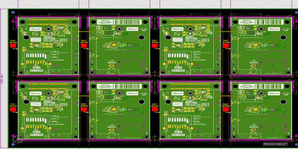
What is a PCB Panel?
Also called panelization PCB, it is a method cojoining or adding more circuit boards into one box. The major advantage to the PCB panel design is savings the costs of making the circuit boards differently.
How to Connect PCB Panel Board
Let us talk about some of the processes or cojoining methods for the panel. The most significant is the use of residual bridges. These bridges have a couple of holes, which aid in the creation of singulation of the circuit boards.
It is important to point out that a couple of factors potentially influence the outcome of the connection. These are:
- The residual bridges, used for connecting the panels or boards, must be positioned or optimized in a way that they create the space for the individual or separate PCBs to be easily disassembled or separated after production.
- Special considerations are worth making for the residual bridges. The core considerations include the determination of the numbers and positioning of the bridges. These help in influencing other metrics that bolster the singulation and stability of the Printed Circuit Boards (PCBs). The metrics include, but are not limited to the circuit board’s thickness, the size of the panel and the positioning of the parts or components on the circuit board.
When You Should Consider Panel Board Design
Note that you don’t necessarily need to make panelized circuit boards if there is no need for it. At Hillman Curtis, we advise our clients on how best to determine the need for the panels.
Here are a few instances on when you should consider making circuit board panels:
1. Expanded Product Design with Limited Budget
Your budget plays a critical role in the quality of the PCB you get. If the budget is not sufficient, you can be sure that the circuits might not turn out to be as expected.
In such instances, it makes sense to figure out better ways to get what you want – even when on a shoestring budget. Luckily, making PCB panels is one of the options on the table. It is an effective way to combine or allow for the pooling/assembling of multiple PCBs into one package.
2. Greater Stability
Making PCB panels can also help in stabilizing the circuits. This is especially so for the flexible-rigid PCBs.
3. Multi-Board Support
PCB panel design also enables the making of different board types into one design. This way, you can use a bit of one circuit board type and the other to make a wholesome PCB.
4. Circuit Board Expansion
Some Printed Circuit Boards (PCBs) need to be expanded or have the sizes extended for reasons, ranging from accommodating more components and meeting up to the manufacturer’s recommended size.
If this is the case, using circuit boards that are smaller in nature doesn’t work. This is why the support of several board type integrations into one panel is an excellent way to enlarge the PCBs that were originally smaller.
5. Defect Prevention
Defects or problems arising from manufacturing potentially hamper the success of many circuit boards. This is why the usage of PCB panel design readily comes in handy when targeting an overall defect prevention or reduction, as the case might be.
This works best when you originally considered working with a smaller PCB. Due to the limited size, in terms of space, you will find that the board wouldn’t fit into the requirements for the alignment holes, fiducials and a host of other Design for Manufacturability (DFM) requirements.
By panelizing the smaller PCBs, you create the channel for the requirements and manufacturing steps to fit into the same board.
The PCB Panel Design Rules to Stick to

One factor that separates the amateurs from the professionals is the extent of the knowledge or insider-information they have about something.
When it comes to the PCB industry, certain rules and guidelines are generally used to validate the Design for Manufacturability (DFM). These rules must be kept in mind when designing the boards, as they help you keep your eyes on the ball.
The following are some of the PCB panel design rules to get the best results from combining many multiple boards:
1. Maintain the Right Board Size
The size of the PCB is an important factor to consider, because it considerably influences the weight and adaptation of the panel.
Ideally, there are two ways to look at this – manually and automated. If you are using the manual method, it is better to use a dimension of 508 x 508 mm. But, if you are using the automated process, you can use the standard 400 x 250 mm board size.
Generally, the lowest you can go with the board size is 50 x 50 mm.
2. Learn How to Optimize the Milled Panel with Positive Bridges
If the panelized PCB uses positive bridges, then it necessitates the need for spacing. This is created in the form of making a small overhauling on the PCB’s edge. It should be created and remained on the edge, only after the circuits have been separated.
3. The Mixed Multiplier Panel Rules
This is the type of circuit board panels that use either milling or scoring to combine or integrate several Printed Circuit Boards (PCBs) into one panel.
If this is to be used, the following mixed multiplier panel guidelines must be followed:
- A minimum distance or spacing of 2 mm should be maintained between the PCB and the milled panels.
- The maximum distance should be 10 mm.
4. Scored Panel Guidelines
The scored panel is a DFM requirement for PCB panels. Unlike the milling process, it doesn’t require spacing.
The only point where a little spacing is usually considered is when the copper areas and conductor lines are to be separated. The recommended spacing is up to 0.5 mm towards the scoring edge. The major reason for spacing these is due to the tolerances encountered when singulating or separating the single circuits.
5. Circuit Board Layout Optimization
The layout of the Printed Circuit Board (PCB) upon which the panels are to be, should not be left out. The layout guidelines dictate how the panels are to be laid out or placed atop the PCB’s surface.
The following are some of the considerations:
- Wave Soldering: if the panels are to be subjected to wave soldering, it is imperative to use the process mostly for the Surface Mount Technology (SMT) components. These components are also to be accordingly aligned to fit into the required orientations for wave soldering.
- Specific Feature Requirements: certain (additional) features are to be integrated or included in the PCBs after the depanelization of the circuits. The term “depanelization” refers to the removal of the Printed Circuit Boards (PCBs) from the panels. Once the circuit boards are due to be depanelized, the next process is to incorporate or use specific features to facilitate the implementation. An understanding of these requirements also aids in the prevention of the damages the circuitry and components are exposed to due to the depanelization process.
- Clearance Extension: it is not ideal to limit the clearances to the depanelization of the PCB’s layout. It should also be extended to the other panel requirements. Doing so helps to reduce the complexities of the process, as well as reducing the time spent resolving some of these challenges that weren’t addressed earlier.
- Perforation Guidelines: the rules on how to make the perforations stipulate, among other things, that the label perforation must not be placed below the label’s center. Sticking to this rule helps in reducing the chances of having protrusion from the PCB’s sides. A better way to position the perforation is by ensuring the placement on each side if it is to be placed between two circuit boards. You can also place it close to the PCB’s edge.
- A special consideration should be in place to mask off the connection point from the protruding components or larger devices that potentially reduce the automated transportation in the production line.
The Methods of Panelizing PCBs
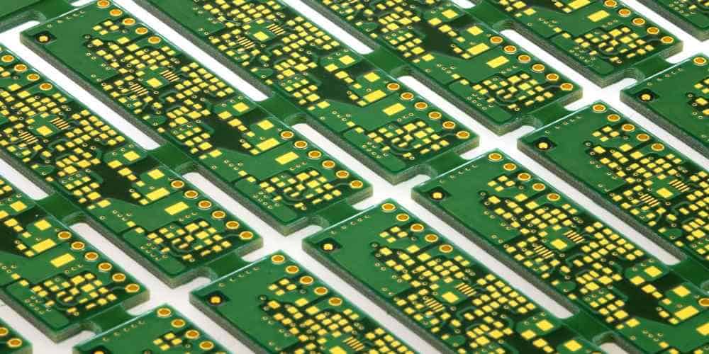
There are different methods for making panelized PCBs, and each is unique. Although the PCB breakaway design and V-scoring are the most outstanding, there are a couple of others.
Here is a breakdown of how each of the circuit board panelization methods work:
1. Tab Routing
Also called the PCB breakaway tabs, they refer to the pre-cutting of the circuit boards from the array. It is then followed up by the use of perforated tabs to hold the PCBs onto the circuit board.
2. V-Scoring
This is another circuit board panelization process. It involves the making of grooves via cutting off from the top and bottom of the PCB, a one-third thickness of the circuit board.
An angled blade is usually used for this process and the remaining third of the PCB is often smoothened out with the help of a machine.
3. Die Cutting
This is the third type of PCB panelization. It entails the punching out of individual PCBs from a panel, with the help of a fixture with die cutter.
4. Solid Tab Panelization for PCBs
It is better to use a laser-cutting machine for this process. It involves making solid tabs between the circuit boards, with the aim of strengthening the bond.
5. Laser Router
Also called the laser-cut PCB panelization method, it involves the automated process of carving or making out any shape from the circuit boards.
In addition to reducing the mechanical stresses that potentially come with the process, laser router also comes in handy when panelizing the PCBs with either unusual shapes or tighter tolerances.
Types of Panels Used for PCB Production
Different types of panels are used to make circuit boards. The choice of these panels ranges from the shapes and sizes. It also includes the specific purpose they serve.
1. Homogenous Composition (AAAA)
Also called the AAAA combination panelization, it entails the making of the same type of PCB on the same panel. This way, you are sure of working with only one type of design.
The benefits include:
- The quality of the printing wouldn’t be reduced during the printed stencil design.
- The AAAA combination panelization of PCBs is always independent of the product portfolio and manufacturing requirements of the different SMT manufacturers.
- It assures of the highest manufacturability across all the panel combinations. This is possible due to the fact that the non-restriction or confiscation of the panelization to the fabrication quantities helps to allow for as many panels to be made.
2. Heterogenous Combination (ABCD)
This is an opposite of the homogenous combination in the sense that it supports the panelization of a wide range of Printed Circuit Boards (PCBs).
In addition to supporting the panelization, i.e., the making of a mix of PCBs at the same time, the heterogenous combination also offers the following benefits:
- It is one of the cost-effective PCB configuration methods, in the sense that it supports the making of different circuit boards on the same panel.
- It is the ideal process to meeting the different requirements of consumer electronics that use a combination of PCBs.
Despite the seeming benefits, using the heterogenous approach to PCB panelization might not be worth it. Among the downsides are the production of larger volumes of PCBs without a demand for the same – and the possible changing of the PCB panel design when modifications are needed.
Wrapping Up
With the PCB panel design, you can be confident of combining multiple circuit board footprints in one package. In addition to protecting the PCB from shock jerks and vibrations, the process also saves time, enables the integration of multiple concepts targeted at different applications and helps in saving the costs on making individual Printed Circuit Boards (PCBs).
