Making circuit boards could be simple or tough, depending on your expertise and the methods you opted to use. Whether you are a beginner or near-professional, one point you mustn’t miss is that the PCB design process has a lot to do with how the board eventually turns out.
A lot of processes go into it, and we have streamlined these into ten (10) major processes. These steps range from the earliest diagraming of the board to the schematic capturing, board layout design and component placement.
What is PCB Design?
It refers to the series of steps involved or taken when making a Printed Circuit Board (PCB). The circuit board, on its part, is a dedicated board that provides the platform for physical/mechanical support and electrical connection of the components via the use of pads and conductive tracks.
At the core of the PCB’s performance is the need to use predesigned copper tracks on a conducting sheet to reduce the number of wires used in the board. This, in extension, helps to reduce the faults resulting from double-verifying and troubleshooting some of the challenges that come with excessive wirings on the breadboard.
1. Validate the Design
The first thing to be done is to be certain of the need for the board. To be on the safe side, you must understand the required electrical parameters and the functions they have on the board’s success.
The needed electrical parameters include but are not limited to the types of circuit components, the locations of these connectors and components, as well as the voltages needed. Other electrical parameters are the shielding considerations, current maximums, impedance characteristics, net wire schematic, types of signals and the capacitance limitations.
2. Draw and Capture the Schematics for Your PCB
Your circuit board is still a bare board, devoid of the mechanical properties needed to make it a working board. To put it in that position, the next step is to draw the schematics. The schematics are more of a graphical representation of what the world would turn out to look like.
From the schematics, you should have an overview of the connections between the groups of circuit components, the types of parts/components to use in the board and the connection paths for these components.
3. Start Creating the PCB Layout
Now that the schematics have been created, it is time to develop the layout of the circuit board based on that.
Have in mind that the successful creation of the layout depends on the type of design tool used and how excellently you maximized the usage. Some of the common circuit board schematic capture tools are KiCad and Altium Designer. Others are Mentor PADS and Allegro.
Here are some of the additional pieces of information about creating a PCB layout with the schematic capture tool:
Footprint Creation
The schematic capture tool, Altium Designer for instance, has a large library of pre-existing component footprints and schematic symbols you can use. However, if you are looking for some adventure, consider making your footprints manually and import the same into the tool.
Schematics Annotation
One of the reasons for annotating the PCB schematics is to enable the easy tracking of the components. Here is how it works:
- The annotation or description should be in the form of name nets. The use of name nets helps to manage larger and complex circuit schematics.
- Use name nets also helps to manage the PCBs with more pin counts. This comes in handy when trying to organize these pins, as well as tracking the connectivity between the circuit board’s components.
- The annotation of the schematics in the form of name nets helps to facilitate the identification of the nets during the routing and placement of the components.
Schematic Linking to the PCB
It is also imperative to link the schematics to the Printed Circuit Board (PCB). This process is imperative to the overall optimization of the board, as the linkage helps to transfer the schematics to the bare board.
Here is what you need to know about linking or connecting/synchronizing the schematics to the PCB design:
- The connection helps the circuit board designer to determine the right fitting for the designated devices/applications.
- Footprint Selection: the type of footprint or process technology has a role to play in the board’s performance. The common options are Through-Hole Technology (THT) and Surface-Mount Technology (SMT). The advantages of the two are the smaller design of the SMT components and the flexible soldering options for the THT. The downsides are that the SMT component footprints are harder because of the smaller design and the THT components are best for beginners.
4. Circuit Board Stackup Design

Your next step is to design the stackup, which includes the types of materials or laminates needed for the PCB design.
The following are some important points to note about the PCB stackup design:
- The PCB stackup considerations should be made at the earliest stage of the board’s design. Here, you want to consider the layer stackup design and the shape the stackup takes.
- The impedance must be considered. It has to do with the pace at which electricity travels down the trace.
- Determine if there is any need for using a differential pair routing in the PCB design.
5. Design Rules and DFM Requirements Definition
At this stage, a serious consideration is given to the specific design rules that could impact how the circuit board functions. These rules often comply with the industry guidelines, especially the standards and acceptability criteria laid down by the IPC.
In addition to choosing to work with a manufacturer that understands these rules, you also want to prioritize the manufacturer’s capabilities in this regard over the years. Hillman Curtis understands how these rules and Design for Manufacturability (DFM) requirements could influence the outcome of the circuit board and electronics manufacturing.
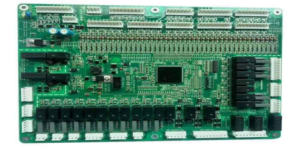
6. PCB Component Placing
It is now the time to place the components on the circuit board. However, it is not expressly done, without considering the following:
- The computation of the datasheets for these components and the sending of the same to the customers for approval before placement.
- Sticking to the layout and design guidelines, especially as they pertain to the proximity of the components.
- It is possible to use the automation capability of the schematic design tool to layout the components on the board.
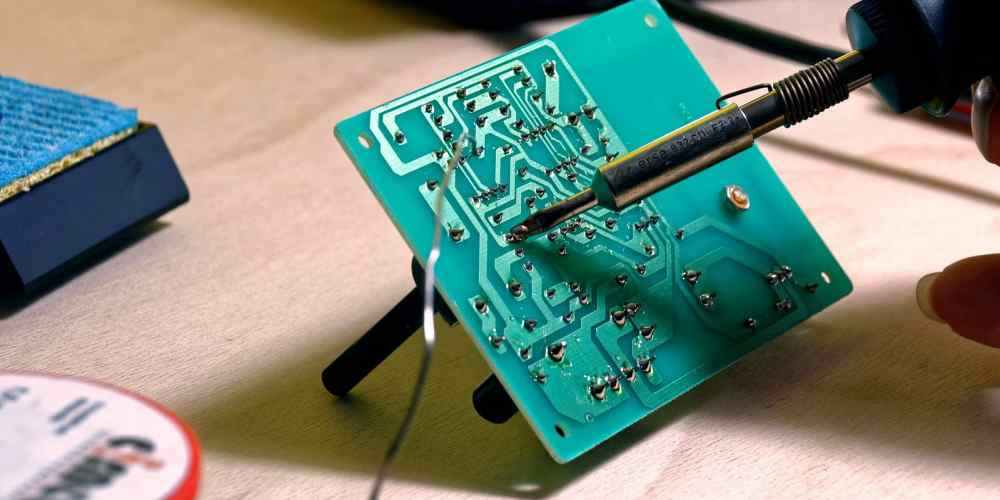
7. Drill Hole Insertion
Now that the holes have been placed, let us now talk about how to insert the drill holes into the board.
The drill holes (including vias and mounting), should be placed before the traces are routed. Take note that the drill hole insertion has a lot to do with the complexity of the board. For instance, a double-sided PCB would need the drill holes need to be connected to the bottom layer.
A simplified process for drill hole insertion is to specify the same in the Design for Manufacturability (DFM) requirements. The specifications as design rules aids the automated placement of the drill holes by the schematic capture tool.
8. Trace Routing
The routing of the traces come next after the mechanical elements and circuit board components have been placed at the appropriate places in the board.
Take note that the routing of the traces has to do with the connection of the segments of the PCB’s paths.
Here are some factors to consider when routing your circuit’s traces:
- The important routes should be connected/routed first. Examples of the important routes are low-level analog signals, power nets and impedance-controlled nets.
- The other (secondary) connections can then be filled after the primary routes have been connected.
9. Integrate the Identifiers and Labels to the PCB
These are the markings that enable the understanding of the different components on the board. In addition to the labels, the other additions to make here are the:
- Logos
- Markings
- Reference Designators: these refer to the specific abbreviations of the PCB components. They aid in the specification of where the components are to be added on the circuit board.
10. Layout and Design Output Files’ Generation
This is usually the final step in the making of circuit boards. The generation of the design output and layout files helps in validating all the processes that have been used in designing the board.
Here are some of the things you need to know about these files:
- Content: the content of these files are usually the pieces of information pertaining to the circuit board’s design.
- The generation of these files now helps the PCB manufacturer to initiate the next processes of fabricating, manufacturing and assembling the circuits.
- DRC: it is best to subject the board to the Design Rule Check (DRC). It works by comparing what you have in the generated files with what you have on the PCB. It is an excellent way of matching the expected outcome/initial conceptualization with what is designed at the end of the day.
Make Your Circuit Boards in Ten Steps
You can see that it is a pretty streamlined process to make PCBs. By following these steps, you stand a better chance to have your PCB design readied.
For the best results and to optimize your boards as per the DFM and design rules requirements, work with us at Hillman Curtis. We use the best schematic capture tool to modify your boards and have the designs readied in a few days. You can also count on us for streamlined and real-time fabrication, circuit manufacturing and assembling of your circuit boards.
