PCB schematic and layout design is a crucial aspect in the development of electronic devices. Schematic design involves creating a visual representation of the circuitry, while layout design involves arranging the components on the board. These two aspects are interdependent and require careful consideration to ensure a functional and reliable end product.
The schematic design stage is where the circuitry is planned out and visualized. This stage involves selecting components and arranging them in a logical and efficient manner. The schematic diagram serves as a blueprint for the layout design, and any errors or oversights here can have major consequences later on. Once the schematic is complete, the layout design can begin.
The layout design stage involves arranging the components on the board in a way that is both functional and efficient. This stage requires attention to detail, as even small errors or oversights can result in malfunctions or failures. The layout design must also take into account factors such as signal integrity, power distribution, and thermal management. By carefully considering these factors, the end product can be optimized for performance and reliability.
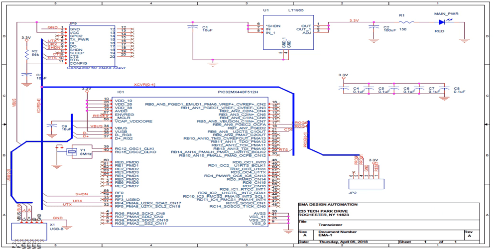
PCB Schematic
When designing a printed circuit board (PCB), creating a schematic is the first step. A schematic is a graphical representation of the electronic components and their interconnections. It provides a clear understanding of the circuit’s functionality, making it easier to design the layout.
Functionality
The schematic diagram shows how the different components of the circuit are connected and how they interact with each other. It provides an overview of the circuit’s functionality, making it easier to identify any potential issues or limitations.
Components
The schematic diagram also provides information about the components used in the circuit. Each component is represented by a symbol that indicates its function and characteristics. The schematic also includes information about the values of the components used, such as resistors, capacitors, and transistors.
Design Tools
There are several design tools available for creating a schematic diagram. Some popular options include Eagle, Altium Designer, and KiCad. These tools provide a user-friendly interface for creating and editing schematics, as well as features such as automatic routing and error checking.
In conclusion, creating a schematic diagram is an essential step in designing a PCB. It provides a clear understanding of the circuit’s functionality and components, making it easier to design the layout. With the help of design tools, creating a schematic diagram has become easier and more efficient than ever before.
PCB Layout
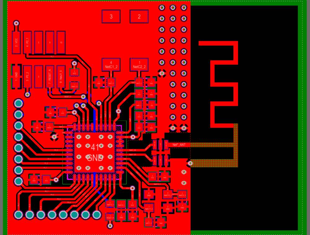
When it comes to designing a PCB, the layout is one of the most important aspects to consider. The layout of a PCB refers to the physical arrangement of the components on the board, as well as the routing of the traces that connect them. Here are some key considerations for PCB layout:
Placement
The placement of components on a PCB is critical to ensuring proper functionality and reliability. Components should be placed in a way that minimizes noise and interference, and allows for efficient routing of traces. Here are some tips for component placement:
- Group components logically based on their function
- Place components in a way that minimizes the length of traces
- Keep high-frequency components as close together as possible
- Leave enough space between components for ease of assembly and maintenance
Routing
Routing is the process of connecting the various components on a PCB with traces. Proper routing is essential for ensuring proper functionality and minimizing noise and interference. Here are some tips for routing:
- Route high-frequency traces first, as they are the most sensitive to noise
- Use wide traces for high-current signals
- Minimize the length of traces to reduce noise and interference
- Route traces in a way that minimizes crosstalk between signals
Design Rules
Design rules are a set of guidelines that define the minimum spacing, trace width, and other parameters for a PCB layout. These rules ensure that the PCB can be manufactured correctly and reliably. Here are some common design rules:
- Minimum trace width and spacing
- Clearance between components and traces
- Minimum drill size and annular ring
- Placement of fiducial markers for assembly
In conclusion, proper PCB layout is critical to ensuring proper functionality and reliability. By following these guidelines for placement, routing, and design rules, you can create a PCB that performs optimally and is easy to manufacture and maintain.
