The design of Printed Circuit Boards (PCBs) starts with the making of the schematics. These are the blueprint of the board, letting the designer know the types of components to be used, the signal routes and where these parts are to be placed on the board.
Considering the importance of the schematic design, you don’t want to make the mistake of not choosing it or following the due processes. In this article, we help you understand all that goes into the making of a PCB schematic design.
What is a PCB Schematic Design?
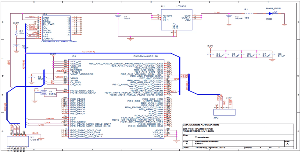
It stands for the “initial design” made for the Printed Circuit Board (PCB). It is a blueprint that signifies the graphical representation of the electronic circuit. With this functional diagram, your circuit designer will have a working diagram that would be used to facilitate the production of the board.
What Goes into Making the PCB’s Schematics?
There are two major applications or productions of the PCB schematics. These are for the flexible and the rigid circuit boards.
On the one hand, we have the flexible PCBs as the circuit boards comprising foldable thin plastic film. The foldability of the flexible PCBs comes in handy for adjusting the circuit board to fit into the tiniest of spaces on the circuit board.
On the other hand, we have the rigid PCBs, which are both non-foldable and hardcore. This means that it doesn’t offer a similar flexibility as the flexible circuit boards do.
Despite the differences in the two, one thing you can be sure of is that the two PCBs follow the same type of schematic design. The difference between the two, however, is that they use a different layout design pattern.
What are the PCB Schematic Design Elements?
Different elements come together to bolster the making of the circuit bord schematics. Understanding how all these works can make all the difference in how you go about making the PCB layout.
The following are some of the elements that are peculiar to the PCB schematic design:
- The thickness of the several traces of the board must be considered, especially as they have to do with the heat dissipation and current generation.
- It is also important to make sure that the components/parts to be used for the board are of the right sizing and that they are positioned in the rightful places on the board’s schematic.
- The schematic must reflect the placement of connectors on the edges of the circuit board.
- Zero Tolerance for Crossing: this should be paid close attention to, because it could negatively impact the signal transmission. It has to do with the assurance of the two connections knitted and that the connections do not cross one another. Even if the crossing must be made, it must not be on the same level, as this could impact the board’s performance. The connection is considered to have crossed if the connections cross one another through any of the following processes: changing or taking a detour to another layer.
- The elements also have to do with the spacing of the components. The spacing or gapping should be done in a way that there should be sufficient space for excellent distribution of heat.
Although the above is some of the core schematic elements, there are others that are as important as they are. These are the wires and the components.
These two are meant to be connected in a way that they would bring forth the desired electrical performance.
When we talk about the components or the footprint (also called the land pattern), we are making a reference to the items we see on the circuit board. These include but are not limited to the collection of Surface-Mount and Through-Hole pads that match the terminal geometry of the physical part of the board.
It is also important to note that the land pattern in the schematic can also have the silkscreen, which combines the following: text, lines and shapes.
On the other hand, we have the wires, which later become the copper pours or traces.
The most important point to note out of all these is that the footprints and the wires basically serve as visual elements. Due to the fact that they lack the conductive elements/capabilities, their presence in the schematic might not affect the circuit’s functionality.
The Core Considerations for PCB Schematic Design

When a mention is made of the schematic design of a circuit board, it is often misinterpreted to be a perfected version of the design. Although this is what the process aims at – helping to set the stage for the circuit’s production, it does come with its flaws.
Therefore, you should not always expect the PCB’s schematic to be free of all the errors. That is why you must have the following points in mind as you get set to make a schematic design for your circuit board:
1. Power Dissipation
What is the board’s capability to dissipate heat after production? By factoring in the heat dissipation on time, you get to avoid some of the issues that arise from it.
2. Impedance Calculation
It is possible that the board wouldn’t live up to expectations, due to the differences identified between the observed impedance and calculated impedance.
This gives us the idea that the impedance used for the PCB’s schematic should try to be as close as possible.
3. Signal Integrity
How signals are transferred or moved across the board is very important. For this reason, check the circuit diagram (schematic) to be sure that it has the signal paths duly laid out for the transmission of signals through the different parts of the PCB.
4. Noise Considerations
How exposed is the PCB going to be to the external noises? These noises tend to cause defects to the board, especially if they are emitted via the Electromagnetic Interference (EMI).
Other factors or considerations that would likely affect the performance and outcome of the circuit include the susceptibility to EMI, the definition of the current return paths on the board, as well as the coupling between the diversified circuit board sections.
5. Signal Track Identification
If there is one feature that shouldn’t be missing in a PCB, it has to be the signal track or route. The need for this includes the highlighting of the pathway for signal flows, as well as identifying where the components are to be placed on that route.
Therefore, the signal tracks or routes must be accurately laid out. Another important to note here is that the signal tracks or routes can be strategically placed on the board, most especially at a little distance or in parts.
Also, note that the placement of the signal tracks must be done in a way that they are in proximity with either the PCB’s physical layout or in conjunction with the board’s layout.
6. Schematic Grouping
It is also possible to group or combine the PCB schematic design into one place. This is commonly deployed when the schematic is being made for the complex circuit boards.
Meeting the Heat and Signal Integrity Requirements
It is important to mention that the integrity of the transmitted signals and the heat dissipation capabilities help to foster the PCB schematic’s optimization for the targeted circuit boards.
It is for this reason that we have to make sure that the signal integrity and heat requirements are met on time. Besides, this should be done faster due to the fact that not all the PCB tracks appear on the same width in the circuit’s layout.
7. Signal Track Division
Just as we are looking to improve the integrity of the signal transmission vias the ideal placements, it is also possible to divide these signal tracks.
The division entails breaking down the signal tracks either into different layers, or by separating and positioning the tracks on both sides of the PCB. Note that the placement of the signal tracks on the PCB’s sides is subject to it being used in either the double-layered or multilayered circuit boards.
The Making of PCB Schematic Design Starts with a CAD Software
When you have decided to use the schematics, it is expedient that you follow the due process. This includes using the right tools, which in this case include the CAD software program.
This wasn’t the case many years ago, when the manual process dominated by making hand-drawing of the schematics was in vogue. Today, you can choose from a plethora of CAD software programs to make your circuit board’s schematics in real-time.
It all boils down to the type of software you choose to work with. If we are to recommend, we would suggest the following:
- KiCAD: this is one of the most popular CAD software programs for making PCB schematic design. It is not only open-source, but relatively affordable and ideal for both beginners and professionals.
- EAGLE: this is another PCB schematic software program. Although it is a bit pricey, you can be sure to use it to design the best schematics for your PCB.
- DesignSpark: just like KiCAD, this is another affordable CAD software program you can use.
- DipTrace: it offers a mixture of intuitive interfacing and affordability. Besides, you can be sure of finding most of the resources needed for PCB schematic design on the program fpga.
What Goes into the Schematic Generation Process?
A wide range of components and components’ attributes are used to make the schematic of a PCB. The following are some of the processes:
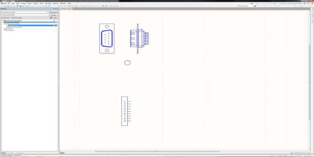
Footprint Assignation
The footprint refers to the components or land pattern used for the design. They must be assigned, as that helps to establish the actual physical size of the components, as well as highlighting where these parts are to be placed or mounted on the PCB’s surface.
The assignation or creation of the footprints often includes the creation of the pads, followed by the detailing of the area and height of the components. The other steps include the keying in of the silkscreen information and the saving of the footprint for later use.
Symbol Generation
This involves the creation of the symbols or component identifiers for the parts on the PCB. The processes involved in generating the symbols include the drawing of the parts’ body, followed by the definition of the reference designators, addition of the pins and the pin numbers and lastly – the assigning of a footprint for the generated symbols.
Symbol Connection
This has to do with the interconnection or joining of the parts in the schematic. The standard practice is to ensure the sharing or interconnection of the electrical connection for the two wires that form a junction in the schematic.
Footprint Linkage
You also need to link or connect the PCB’s footprint to the generated symbols. Doing this enables the transfer of the schematic information/data to the Printed Circuit Board (PCB)’s layout.
Reference Designators Placement
These are the dedicated letters and numbers used to denote the type of component or part used on the PCB. It also indicates the components’ supplier, value, manufacturer, and part number.
The standard practice is to use the industry-related designation for such components. For example, the letter “R” is the reference designator for resistors. Another standard practice is to make sure the components are labelled accordingly or alphabetically.
Final Words: Are there Differences between PCB Schematic and PCB Design?
Some circuit board consumers are sometimes unsure if there are differentiators between the PCB schematic and the circuit board design.
First, the schematic has to do with the blueprint – a background information required for starting the board development. It is only after the schematic has been drawn or made that the next stage of designing the board starts.
Another difference between the two is that the circuit board schematic shows the functionality and connectivity existing between the different PCB components, while the PCB design has to do with where these components are to be placed on the board.
In conclusion, the PCB schematic and PCB design work hand-in-hand to enable the development of a circuit board. Always contact a reliable PCB contract manufacturer in the name of Hillman Curtis to handle the tasks for you.
