Printed circuit board (PCB) design is an essential part of the electronics industry, as it is the foundation of all electronic devices. PCBs are used to connect electronic components, such as resistors, capacitors, and transistors, to create a functioning circuit. The design of the PCB is critical to the success of the product, as it determines the performance, reliability, and cost of the device.
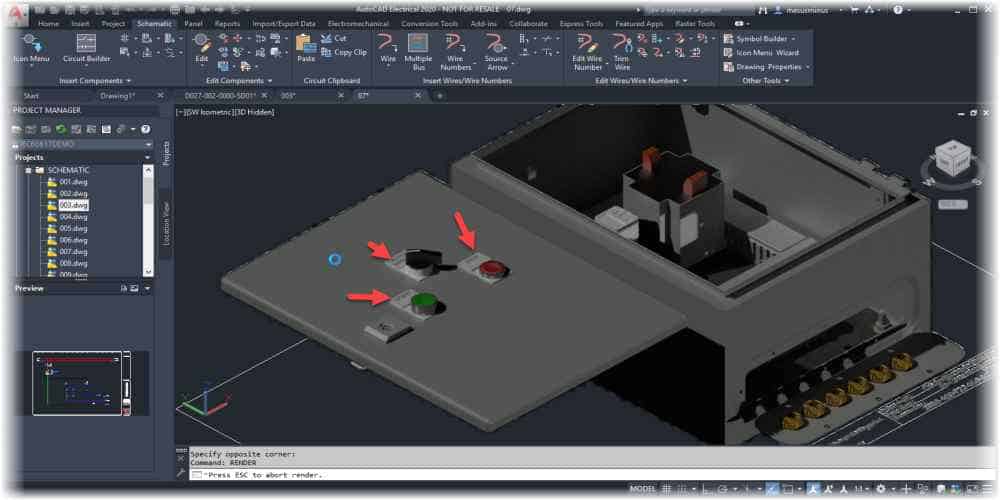
AutoCAD is a popular computer-aided design (CAD) software used in the electronics industry for PCB design. AutoCAD provides a user-friendly interface and powerful tools to design complex PCB layouts. The software allows users to create schematic diagrams, place components, and route traces, all in a single environment. AutoCAD also provides advanced features, such as design rule checking and 3D visualization, to ensure that the design meets the required specifications.
Autocad Basics
Interface and Tools
Autocad is a computer-aided design (CAD) software used by engineers and designers to create 2D and 3D models. The software has a user-friendly interface with a variety of tools that help in the design process. The interface consists of the following elements:
- Menu Bar: Contains various commands and options for creating, editing, and managing drawings.
- Toolbar: Provides quick access to frequently used commands.
- Command Line: Displays the current command being executed and prompts the user for input.
- Drawing Area: The main workspace where the drawing is created.
Creating a New Project
To create a new project in Autocad, follow these steps:
- Open Autocad and select “New Drawing” from the “Start” tab.
- Choose the drawing template that suits your project requirements.
- Set the units of measurement for the drawing.
- Save the drawing with a suitable name and location.
Drawing and Editing Tools
Autocad provides a wide range of drawing and editing tools that enable designers to create accurate and detailed drawings. Some of the commonly used tools are:
- Line: Creates a straight line between two points.
- Circle: Creates a circle with a specified radius.
- Arc: Creates an arc with a specified radius and angle.
- Rectangle: Creates a rectangle with a specified length and width.
- Trim: Removes parts of a drawing that are not required.
- Extend: Extends a line or an arc to meet another object.
In addition to these tools, Autocad also provides advanced features like layers, blocks, and dimensions that help in organizing and annotating the drawing.
Overall, Autocad is a powerful tool for printed circuit board design that offers a range of features and tools to create accurate and detailed drawings.
PCB Design Process

The printed circuit board (PCB) design process involves several steps that must be followed to ensure the final product meets the required specifications. This section will discuss the four main stages of the PCB design process using AutoCAD software.
Schematic Design
The schematic design is the first stage of the PCB design process. It involves creating a graphical representation of the circuit using symbols and connecting lines. This stage helps to identify the components needed for the circuit and how they will be connected.
Component Placement
Once the schematic design is complete, the next stage is component placement. This stage involves placing the components on the PCB layout. The placement of components can affect the performance of the circuit, so it is essential to place them correctly.
Routing and Tracing
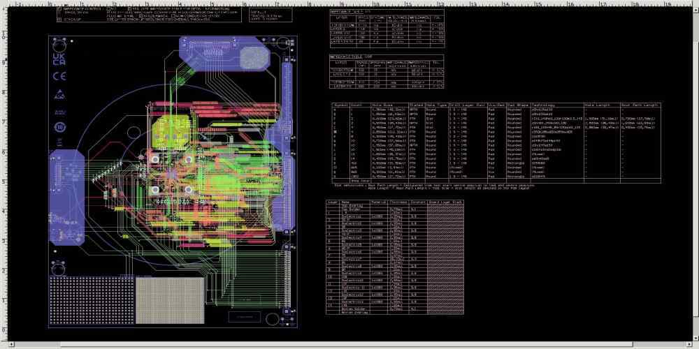
The routing and tracing stage involves creating the physical connections between the components using copper traces. This stage requires careful consideration of the trace width, spacing, and direction to ensure the circuit’s proper functioning. AutoCAD software provides several routing options, including manual and automatic routing.
Design Rule Check
The final stage of the PCB design process is the design rule check. It involves checking the design against specific rules and constraints to ensure that the PCB meets the required specifications. This stage helps to identify any errors or issues that may affect the circuit’s performance.
In conclusion, the PCB design process involves several steps that must be followed to ensure the final product meets the required specifications. AutoCAD software provides various tools and features to assist in the design process, making it easier to create high-quality PCB designs.
Advanced Techniques
Multi-Layer PCB Design
Multi-layer PCBs are used to increase the density of components and reduce the size of the board. In Autocad, you can design multi-layer PCBs by using the “Layer” command. The “Layer” command allows you to create multiple layers and assign different properties to each layer. This helps in separating the components and tracks on different layers, making it easier to design and manufacture the board.
Signal Integrity Analysis
Signal integrity is one of the critical aspects of PCB design. Signal integrity analysis ensures that the signals transmitted through the board are not distorted or lost. In Autocad, you can perform signal integrity analysis using the “Analyze” command. The “Analyze” command allows you to analyze the signal traces, identify any issues, and optimize the design for better signal integrity.
Thermal Management
Thermal management is essential to ensure that the components on the board do not overheat and fail. In Autocad, you can design thermal management systems by using the “Thermal” command. The “Thermal” command allows you to create thermal vias, thermal pads, and copper pours to dissipate heat away from the components.
Manufacturing and Assembly
Manufacturing and assembly are critical aspects of PCB design. In Autocad, you can design the board for manufacturing and assembly by using the “Design Rules” command. The “Design Rules” command allows you to set up design rules for the board, such as minimum trace width, minimum clearance, and minimum drill size. This ensures that the board can be manufactured and assembled correctly.
Overall, Autocad provides advanced techniques for designing printed circuit boards. By using the multi-layer PCB design, signal integrity analysis, thermal management, and manufacturing and assembly features, you can design high-quality PCBs that meet your project’s requirements.
Tips and Tricks
Keyboard Shortcuts
Using keyboard shortcuts in Autocad can significantly speed up your PCB design process. Here are some useful shortcuts for PCB design:
- F8: Turn on/off Ortho mode
- F9: Turn on/off Snap mode
- F3: Turn on/off Object Snap mode
- F4: Turn on/off Object Snap Tracking
- CTRL + C: Copy selected object(s)
- CTRL + V: Paste copied object(s)
- CTRL + Z: Undo last action
- CTRL + A: Select all objects
- CTRL + SHIFT + C: Copy to clipboard with base point
- CTRL + SHIFT + V: Paste from clipboard with base point
Customizing Autocad for PCB Design
Customizing Autocad for PCB design can make your workflow more efficient. Here are some tips:
- Create custom toolbars with frequently used commands to access them quickly.
- Set up layers with specific colors and line types to differentiate between different components and nets.
- Use block libraries to save time and maintain consistency in your designs.
- Use templates to set up your drawing with specific units, scales, and grid settings.
Troubleshooting
When designing PCBs in Autocad, you may encounter some issues. Here are some common problems and solutions:
- Problem: Objects are not snapping to the grid.
- Solution: Make sure Snap mode is turned on and that the grid is visible. Check the grid settings to ensure that the spacing is correct.
- Problem: Layers are not displaying correctly.
- Solution: Check the layer settings to ensure that the correct layers are turned on and that the colors and line types are correct.
- Problem: Objects are not copying or pasting correctly.
- Solution: Check that the correct objects are selected and that the copy and paste commands are being used correctly.
By using these tips and tricks, you can improve your PCB design process in Autocad.
