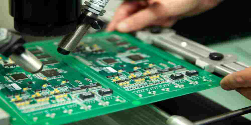
Printed circuit board (PCB) layout design is an essential aspect of the electronics industry. PCBs are used in a wide range of devices, from smartphones to medical equipment, and their layout design plays a critical role in the performance and functionality of these devices.
The PCB layout design process involves placing components on a board and routing traces between them to create an electrical circuit. Designers must consider factors such as signal integrity, power distribution, and thermal management to ensure that the circuit operates correctly and reliably.
Effective PCB layout design requires a combination of technical knowledge, creativity, and attention to detail. Designers must have a thorough understanding of the components and their specifications, as well as the principles of circuit design. They must also consider the physical constraints of the PCB, such as size, shape, and placement of components, to optimize the layout for performance and manufacturability.
Basics of PCB Layout Design
Understanding PCB Layout Design
Printed Circuit Board (PCB) layout design is the process of arranging components and creating connections on a PCB. It is an essential step in the manufacturing of electronic devices. The PCB layout design determines the performance, reliability, and cost of the final product. A well-designed PCB layout can reduce interference, improve signal integrity, and increase the lifespan of the product.
Components of PCB Layout Design
The components of a PCB layout design include the following:
- Components: The electronic components that will be mounted on the PCB, such as resistors, capacitors, and integrated circuits.
- Traces: The conductive paths that connect the components on the PCB. The width, spacing, and length of the traces affect the electrical characteristics of the circuit.
- Pads: The metal areas where the components are soldered onto the PCB.
- Vias: The holes that connect the different layers of the PCB.
- Silkscreen: The markings on the PCB that indicate the component names, values, and polarity.
Tools for PCB Layout Design
There are many tools available for PCB layout design, ranging from free to expensive. Some of the popular tools include:
- Eagle PCB Design: A free and open-source tool that is suitable for small to medium-sized projects.
- Altium Designer: A professional tool that is widely used in the industry. It has advanced features for complex designs.
- KiCAD: A free and open-source tool that is suitable for small to medium-sized projects. It has a user-friendly interface and a large community for support.
In conclusion, PCB layout design is a crucial step in the manufacturing of electronic devices. Understanding the components and tools involved in the process is essential to create a well-designed and reliable PCB layout.
PCB Layout Design Process
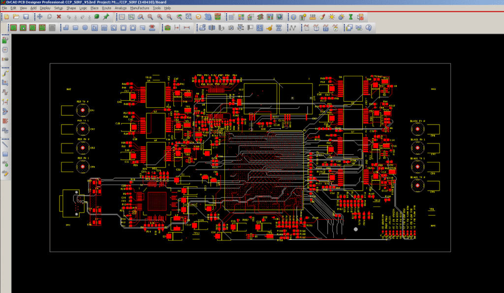
When designing a Printed Circuit Board (PCB), the layout design process is crucial to ensure that the final product functions as intended. The process involves several steps, including schematic capture, component placement, routing, and design rule check.
Schematic Capture
The first step in the PCB layout design process is schematic capture. This involves creating a diagram that represents the electrical connections between the components of the circuit. The schematic is used as a reference throughout the design process to ensure that the layout matches the intended circuit design.
Component Placement
After the schematic is created, the next step is component placement. This involves deciding where each component will be placed on the PCB. The placement of components is critical to ensure that the circuit functions as intended and that there is enough space for routing the traces.
Routing
Once the components are placed, the next step is routing. This involves creating the physical connections between the components using copper traces. The routing process should be done carefully to avoid interference between the traces and to ensure that the circuit functions as intended.
Design Rule Check
After routing is complete, the final step is the design rule check. This involves checking the design against a set of rules that ensure that the PCB is manufacturable and that it meets the required specifications. The design rule check should be done carefully to avoid errors that could cause the circuit to fail.
In conclusion, the PCB layout design process is critical to ensure that the final product functions as intended. The process involves several steps, including schematic capture, component placement, routing, and design rule check. By following these steps carefully, designers can create a PCB that meets the required specifications and functions as intended.
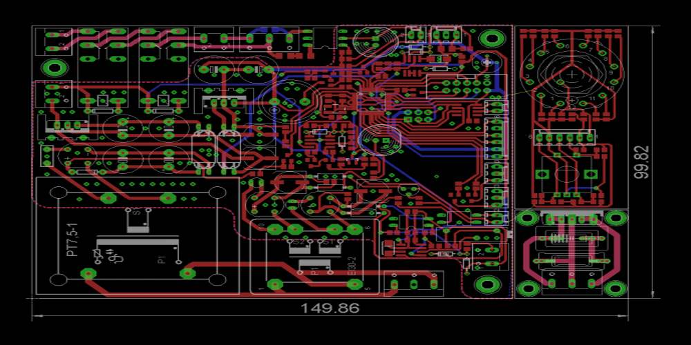
Considerations for PCB Layout Design

Signal Integrity
Signal integrity is a crucial aspect of PCB layout design that ensures the signal quality is maintained throughout the circuit. To achieve good signal integrity, the following considerations should be kept in mind:
- Minimize the length of high-speed signal traces
- Use proper termination techniques for high-speed signals
- Keep analog and digital signals separated
- Avoid routing signals over split planes or gaps in planes
- Use controlled impedance traces for high-speed signals
Power and Ground Planes
Power and ground planes are essential for providing a stable power supply and minimizing noise in the circuit. The following considerations should be taken into account when designing power and ground planes:
- Use multiple power and ground planes to reduce noise
- Keep the power and ground planes close together to reduce inductance
- Place decoupling capacitors close to the power pins of ICs
- Avoid routing signals over the split planes or gaps in planes
Thermal Management
Thermal management is necessary to ensure that the PCB operates within safe temperature limits. The following considerations should be kept in mind while designing for thermal management:
- Place heat-generating components away from each other
- Use thermal vias to dissipate heat from the board
- Use thermal relief pads for high-current components
- Use copper pours to dissipate heat
EMI/EMC Compliance
EMI/EMC compliance is necessary to ensure that the PCB does not interfere with other devices or is not susceptible to interference. The following considerations should be kept in mind while designing for EMI/EMC compliance:
- Keep the signal traces short and straight
- Use proper grounding techniques
- Use shielding for sensitive components
- Use EMI/EMC filters where necessary
By keeping these considerations in mind, PCB designers can ensure that their designs meet the required specifications and perform reliably.
Advanced PCB Layout Design Techniques
High-Speed Design
High-speed signals require careful consideration during PCB layout design. The following techniques can be used to ensure signal integrity:
- Use controlled impedance traces to match the characteristic impedance of the transmission line.
- Minimize the length of high-speed traces to reduce signal reflection and attenuation.
- Place decoupling capacitors close to the power pins of high-speed components to provide a low-impedance path for high-frequency noise.
RF Design
RF circuits require special attention to minimize signal loss and interference. The following techniques can be used to achieve good RF performance:
- Use a ground plane to provide a low-impedance return path for RF signals.
- Place components close to each other to minimize the length of RF traces.
- Use a microstrip or stripline transmission line to maintain a constant impedance.
Flex and Rigid-Flex Design
Flex and rigid-flex PCBs are becoming increasingly popular due to their flexibility and space-saving benefits. The following techniques can be used to ensure reliable operation of flex and rigid-flex PCBs:
- Use flexible materials with good mechanical properties to avoid cracking and tearing.
- Minimize the number of flex-to-rigid transitions to reduce stress on the flexible material.
- Use proper bending radius to avoid damaging the flexible material.
Mixed-Signal Design
Mixed-signal circuits require careful consideration of both analog and digital signals. The following techniques can be used to minimize noise and interference:
- Separate analog and digital ground planes to avoid coupling between them.
- Use a guard ring around sensitive analog components to reduce noise.
- Use differential signaling to minimize common-mode noise.
In conclusion, advanced PCB layout design techniques are essential for achieving reliable and high-performance PCBs. By using the techniques outlined above, designers can ensure signal integrity, reduce interference, and improve overall performance.
