Table of Contents
TogglePrinted circuit board (PCB) prototypes are essential components in the electronics industry. They are used to test and validate designs before mass production. A PCB prototype is a working model of a circuit board that is created to test the functionality and performance of a design. This process allows designers to identify and correct any issues before the final product is produced.
Creating a PCB prototype involves several steps, including design, fabrication, and assembly. The design process involves creating a schematic and a layout of the circuit board. The schematic is a diagram that shows the electrical connections between components, while the layout is a physical representation of the board. Once the design is complete, the fabrication process begins. This involves printing the circuit board onto a substrate, such as fiberglass or plastic, and etching away the unwanted copper. Finally, the components are assembled onto the board using a soldering process. The end result is a working prototype that can be tested and refined before mass production.

Benefits of Printed Circuit Board Prototypes
Printed Circuit Board (PCB) prototypes are an essential part of the product development process. They offer several benefits that make them an ideal choice for engineers and designers. Here are some of the key benefits of using PCB prototypes:
-
Cost-effective: PCB prototypes are a cost-effective way to test and validate a design before moving to mass production. They allow engineers to identify and fix any design flaws early on, reducing the risk of expensive rework later.
-
Faster time-to-market: PCB prototypes can be produced quickly, allowing designers to test and iterate their designs rapidly. This faster time-to-market can be a significant competitive advantage, especially in industries where speed is critical.
-
Improved design quality: PCB prototypes allow designers to test and refine their designs before committing to mass production. This iterative process can lead to improved design quality and better overall product performance.
-
Customization: PCB prototypes can be customized to meet specific design requirements. This flexibility allows designers to create unique products that stand out in the market.
-
Reduced risk: PCB prototypes help reduce the risk of product failure by identifying and fixing design flaws early on. This early testing can save time and money in the long run and prevent potential safety issues.
In summary, PCB prototypes offer several benefits that make them an essential part of the product development process. They are cost-effective, fast, customizable, and can improve design quality while reducing risk.
Types of Printed Circuit Board Prototypes

Printed circuit board prototypes are essential in the development of electronic devices. They allow engineers to test and refine their designs before moving on to mass production. There are several types of PCB prototypes available, each with its own advantages and disadvantages.
Single-Sided PCB Prototypes
Single-sided PCB prototypes are the simplest and most common type of PCB prototype. They have conductive material on only one side of the board, which limits their complexity but also makes them less expensive to produce. Single-sided PCBs are suitable for simple circuits and are often used in consumer electronics.
Double-Sided PCB Prototypes
Double-sided PCB prototypes have conductive material on both sides of the board, which makes them more complex and versatile than single-sided PCBs. They are suitable for more complex circuits and can be used in a wide range of electronic devices. Double-sided PCBs are more expensive than single-sided PCBs but are still relatively affordable.
Multilayer PCB Prototypes
Multilayer PCB prototypes have multiple layers of conductive material and insulation, which makes them even more complex and versatile than double-sided PCBs. They are suitable for the most complex circuits and are often used in high-end electronic devices such as smartphones and computers. Multilayer PCBs are the most expensive type of PCB prototype, but they offer the most flexibility and performance.
In conclusion, the type of PCB prototype you choose will depend on the complexity of your circuit and your budget. Single-sided PCBs are the most affordable but are limited in their complexity, while multilayer PCBs offer the most flexibility and performance but are the most expensive. Double-sided PCBs offer a good balance between cost and complexity and are suitable for a wide range of electronic devices.
Factors to Consider When Choosing a Printed Circuit Board Prototype Service

When choosing a printed circuit board prototype service, there are several factors that you should consider to ensure that you select the best service provider for your needs. Here are some of the most important factors to consider:
1. Quality
The quality of the printed circuit board prototype is crucial to the success of your project. You need to ensure that the service provider uses high-quality materials and follows strict quality control procedures to produce a reliable and durable PCB prototype.
2. Turnaround Time
The turnaround time is another important factor to consider when choosing a PCB prototype service. You need to ensure that the service provider can deliver the prototype within the required timeframe to avoid delays in your project.
3. Cost
The cost of the PCB prototype service is also an important consideration. You need to ensure that the service provider offers competitive pricing without compromising on the quality of the prototype.
4. Technical Expertise
The technical expertise of the service provider is also crucial to the success of your project. You need to ensure that the service provider has the necessary skills and experience to produce a high-quality PCB prototype that meets your specific requirements.
5. Customer Support
Finally, you need to consider the level of customer support provided by the service provider. You need to ensure that the service provider offers excellent customer support to address any issues or concerns that may arise during the PCB prototype production process.
In summary, when choosing a printed circuit board prototype service, you need to consider the quality of the prototype, the turnaround time, the cost, the technical expertise of the service provider, and the level of customer support provided. By considering these factors, you can select the best service provider for your needs and ensure the success of your project.
Steps Involved in Creating a Printed Circuit Board Prototype

Creating a printed circuit board (PCB) prototype involves several steps, each of which is crucial to the success of the final product. Here are the steps involved in creating a PCB prototype:
-
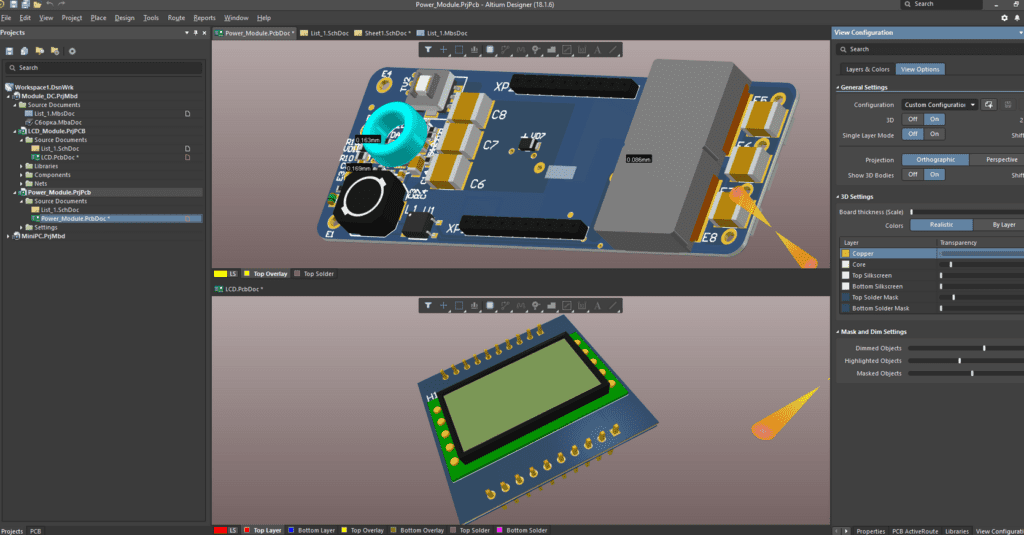
Design the Schematic: The first step in creating a PCB prototype is to design the schematic of the circuit. This is a graphical representation of the circuit that shows how the components are connected. The schematic is created using software like Eagle or Altium Designer.
-
Create the Layout: The next step is to create the layout of the PCB. This involves placing the components on the board and routing the traces that connect them. The layout is also created using software like Eagle or Altium Designer.
-
Generate Gerber Files: Once the layout is complete, the next step is to generate Gerber files. These files contain all the information needed to manufacture the PCB, including the location of the components, the routing of the traces, and the drill holes.
-
Order PCBs: After the Gerber files are generated, the next step is to order the PCBs. There are many PCB manufacturers that offer prototype PCB services, including OSH Park and Seeed Studio.
-
Assemble the PCB: Once the PCBs are received, the next step is to assemble the components onto the board. This can be done manually or using automated assembly equipment.
-
Test the PCB: The final step is to test the PCB to ensure that it works as expected. This can be done using a multimeter or an oscilloscope.
Creating a PCB prototype can be a challenging process, but by following these steps, you can ensure that your final product is of high quality and meets your specifications.
Common Mistakes to Avoid When Creating a Printed Circuit Board Prototype

Creating a printed circuit board prototype can be a challenging task, especially for beginners. Even experienced designers can make mistakes that can lead to wasted time, money, and effort. In this section, we will discuss some common mistakes that you should avoid when creating a printed circuit board prototype.
1. Not Checking the Design Rules
One of the most common mistakes is not checking the design rules before starting the layout. Design rules are specific parameters that define the minimum and maximum values for various aspects of the PCB, such as trace width, spacing, and clearance. Not following these rules can lead to problems such as short circuits, signal interference, and manufacturing defects.
2. Not Considering the PCB Stackup
Another mistake is not considering the PCB stackup. The stackup refers to the arrangement of the layers that make up the PCB. Each layer has a specific purpose, such as power, ground, or signal routing. Not considering the stackup can lead to problems such as signal loss, crosstalk, and electromagnetic interference.
3. Using Inadequate Trace Widths
Using inadequate trace widths is another common mistake. Trace width is the width of the copper traces on the PCB. Using too narrow traces can lead to problems such as high resistance, voltage drop, and overheating. It is important to use appropriate trace widths based on the current-carrying capacity of the trace.
4. Not Checking for Design Rule Violations
Not checking for design rule violations is another mistake. Design rule violations occur when the layout does not comply with the design rules. It is important to check for violations before sending the design for manufacturing. Most PCB design software has a design rule check feature that can help detect violations.
5. Not Testing the Prototype
Finally, not testing the prototype is a mistake that can lead to problems in the final product. Testing the prototype can help detect problems such as incorrect connections, short circuits, and signal integrity issues. It is important to test the prototype thoroughly before moving on to the final product.
In conclusion, creating a printed circuit board prototype requires careful planning and attention to detail. By avoiding these common mistakes, you can save time, money, and effort and ensure a successful outcome.

