In the world of electronic design and manufacturing, PCB prototypes play a significant role in ensuring the success of your project. A PCB, or printed circuit board, is a vital component found in nearly all electronic devices. It mechanically supports and electrically connects electrical components within the device. The importance of a well-designed PCB cannot be overstated, as it directly impacts the functionality and reliability of the product.
Opting for a PCB prototype is an essential step in the design process. A prototype is a preliminary model of the final PCB design that serves as a proof of concept, allowing engineers to test and validate the design before moving towards mass production. This stage enables designers to identify any potential issues or improvements needed, ultimately saving time, money, and resources. It is crucial to invest in a PCB prototype to ensure that your end-product is both efficient and reliable.
The need for PCB prototypes extends to various industries, from consumer electronics to medical devices and aerospace technology. Leveraging the benefits of a prototype can help companies avoid costly design errors and prevent potential inconsistencies in the final product. By investing in a PCB prototype, developers can streamline the development process, make necessary adjustments, and optimize their product for success in the market.
What Is a PCB Prototype
A PCB prototype is an early version or sample of a printed circuit board (PCB) that is created for the purpose of testing and refining the design before mass production. This preliminary stage is crucial for detecting any potential issues or challenges in the design, functionality, or manufacturing processes.
There are several factors that influence the choice of materials and components in a PCB prototype, including:
- Functionality: the intended use of the PCB, such as in a specific electronic application or system
- Design constraints: physical limitations imposed by the component layout or other design specifications
- Cost: budget considerations for the overall project, influencing the choice of materials and components
- Performance requirements: electrical, thermal, or mechanical performance needs of the PCB
PCB prototypes typically undergo various testing methods to ensure their quality and reliability. These methods include:
- Visual Inspection: checking for any visible defects or inconsistencies in the PCB design
- Electrical Testing: measuring the continuity and resistance of the board’s circuits to ensure they meet design specifications
- Functional Testing: making sure the prototype functions as intended in its target application or system
By producing a PCB prototype before moving to full-scale production, engineers can save both time and resources by identifying and resolving any design flaws early on. Additionally, prototyping allows for performance optimization, resulting in a more efficient final product.
Benefits of PCB Prototypes
Error Detection and Correction
One of the main advantages of using PCB prototypes is their ability to detect and correct errors. Mistakes in circuit designs can lead to functional or safety issues, which can result in expensive recalls and redesigns. By prototyping the PCB, engineers can test and validate the design while making necessary modifications early in the process. This saves time and money while reducing the likelihood of future issues.
Design Flexibility
Another benefit of PCB prototypes is the design flexibility they offer. Creating a prototype does not require the same level of commitment as a production run, so designers can experiment with different layouts, component placements, and materials to optimize their designs. If modifications are made, they can quickly create a new version of the PCB without incurring significant costs. This iterative process allows engineers to fine-tune their designs for performance, cost, and manufacturability.
Cost-Effectiveness
PCB prototypes can lead to significant cost savings, as they help to eliminate the need for redesigning boards later in the production process. By identifying design flaws and functionality issues early, costs associated with rework and scrap materials can be reduced. Additionally, optimized designs result in fewer problems during production, which directly reduces costs and time spent in the manufacturing process.
To illustrate the cost-effectiveness of prototyping, consider the following example:
| Item | Non-Prototyping PCB | Prototyping PCB |
|---|---|---|
| Initial Design Cost | $5,000 | $5,000 |
| Revision Cost (due to errors) | $10,000 | $1,000 |
| Production Cost | $100,000 | $100,000 |
| Total Cost | $115,000 | $106,000 |
In this scenario, prototyping the PCB results in a $9,000 savings by reducing revision costs. This makes it clear that PCB prototypes are a cost-effective solution for refining designs and avoiding potential production issues.
PCB Prototype Manufacturing Process

Design and Layout
The first step in the PCB prototype manufacturing process is the design and layout. This involves creating a schematic diagram of the circuit, which outlines the electronic components and their connections. Designers use computer-aided design (CAD) software to create the schematic and layout.
Once the schematic is complete, the next step is converting the schematic into a physical layout. This involves placing components on a virtual grid and routing the electrical connections, forming the copper conductive traces. Designers ensure that the layout adheres to design rules and industry standards to prevent manufacturing issues and improve the overall performance of the PCB.
Fabrication
After the design and layout are finalized, the fabrication process begins. Several steps are involved in the fabrication process:
-
Copper Cladding and Imaging: The base material, typically a rigid fiberglass substrate such as FR4, is clad with thin copper sheets on both sides. A layer of photoresist material is then applied, and the PCB layout is transferred onto the copper using a photolithographic process.
-
Etching: The exposed copper is removed using a chemical solution, leaving behind the desired copper traces.
-
Drilling: Holes for through-hole components, vias, and mounting are drilled into the PCB based on the layout design.
-
Plating: A thin layer of copper is electroplated onto the exposed walls of the drilled holes to ensure electrical conductivity.
-
Solder Mask and Silkscreen: A protective solder mask is applied to the PCB, exposing only component pads and copper traces. A silkscreen layer is then added, displaying component indicators, logos, and other important information.
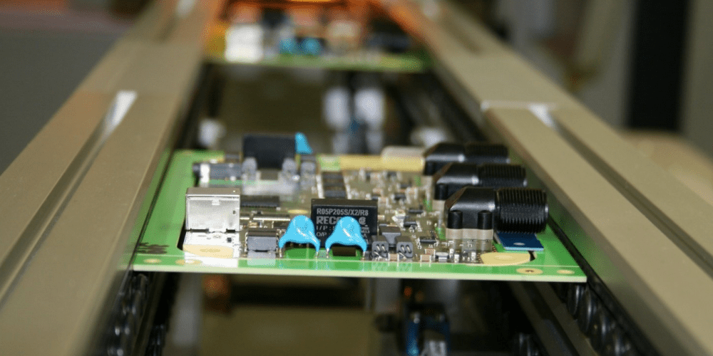
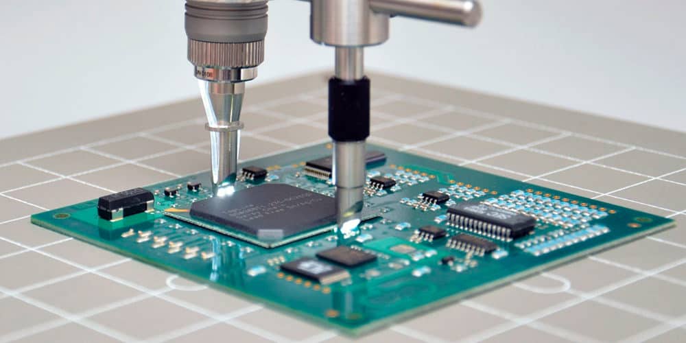
Assembly
The final stage of PCB prototype manufacturing is assembly, which involves attaching electronic components to the PCB. There are two primary methods of assembly:
-
Through-Hole Assembly: Components with leads are inserted into drilled holes and soldered to the corresponding copper pads on the PCB. This method provides strong mechanical bonding and is suitable for high-reliability applications.
-
Surface Mount Assembly: Components with small metal tabs, or leads, are positioned on copper pads and soldered using a reflow process. This method allows for smaller component sizes, greater component density, and improved automation.
Once all components are securely attached to the PCB, the prototype undergoes testing and verification to ensure correct functionality before moving to full-scale production.
Selecting the Right PCB Prototype Service
Quality and Experience
When choosing a PCB prototype service, it is crucial to consider the quality of their work and their experience in the industry. You can verify their expertise by checking for:
- Industry certifications and quality standards compliance, such as ISO and IPC
- Years of experience in PCB prototyping and manufacturing
- Client testimonials and case studies of previous projects
- The range of PCB technologies and materials they support
Turnaround Time
Another important factor is the turnaround time of the PCB prototype service. Assess their lead times and ensure that it aligns with your project deadlines. Some services offer expedited services for an additional cost. In general, look for a provider with:
- Competitive and transparent lead times
- Expedited services for urgent projects
- Reliable on-time delivery performance
Customer Support
Last but not least, consider the customer support provided by the PCB prototype service. Effective communication and support are vital to the success of your PCB project. When evaluating customer support, consider the following:
- Availability of technical support throughout the production process
- Responsiveness to queries via multiple communication channels (phone, email, chat, etc.)
- Providing a dedicated account manager or support for complex projects
- Offering value-added services, such as design review and component sourcing
Conclusion
A PCB prototype serves as a crucial step in the development of electronic products. It helps engineers and designers identify and address potential problems in the design phase, reducing the risk of costly manufacturing errors. Furthermore, PCB prototyping enables faster product cycle times by allowing for rapid design iterations and testing.
- Cost-effective and efficient production
- Faster time to market
- Improved product quality
Implementing a PCB prototype can save businesses both time and resources and benefit end-users with reliable, high-quality electronic devices. Remember to work with reputable PCB manufacturers for a smooth prototyping process and optimal results.
