Printed circuit designers play a crucial role in the electronics industry. They are responsible for designing and creating the blueprints for printed circuit boards (PCBs) that are used in a wide range of electronic devices. PCBs are essential components in electronic devices ranging from smartphones to medical equipment, and they are used to connect and control the flow of electricity between different components.
Printed circuit designers must have a deep understanding of electronics and the ability to design circuit boards that are efficient, reliable, and cost-effective. They use specialized software to create detailed schematics and layouts of PCBs, taking into account factors such as the size and shape of the board, the number of components that need to be connected, and the requirements of the device the board will be used in. Once the design is complete, the designer works closely with manufacturers to ensure that the PCB is produced to the required specifications.
In recent years, the demand for printed circuit designers has grown significantly, as the electronics industry continues to expand and new technologies emerge. As a result, there are many opportunities for individuals with the right skills and knowledge to pursue a career in this field. Whether working for a large electronics manufacturer or as a freelance designer, printed circuit designers play a vital role in bringing electronic devices to life.

Job Overview
Printed circuit designers are responsible for designing and developing printed circuit boards (PCBs) for various electronic devices. They work with engineers and other professionals to create PCB layouts that meet the requirements of the device and ensure that the boards are produced efficiently and effectively.
Responsibilities
Printed circuit designers are responsible for a variety of tasks related to the design and development of PCBs. Some of their main responsibilities include:
- Collaborating with engineers and other professionals to understand the requirements of the device and design PCB layouts that meet those requirements
- Creating and modifying PCB designs using computer-aided design (CAD) software
- Conducting tests and simulations to ensure that the PCB designs are functional and meet performance standards
- Identifying and resolving any issues or problems with the PCB designs
- Working with manufacturers to ensure that the PCBs are produced efficiently and effectively
Skills and Qualifications
To be a successful printed circuit designer, there are several skills and qualifications that are necessary. These include:
- A strong understanding of electrical engineering principles and concepts
- Proficiency in computer-aided design (CAD) software, particularly software used for PCB design
- Excellent problem-solving skills and attention to detail
- Strong communication and collaboration skills, as printed circuit designers often work closely with engineers, manufacturers, and other professionals
- A bachelor’s degree in electrical engineering, computer engineering, or a related field is typically required
Overall, printed circuit designers play a critical role in the development of electronic devices. With their expertise in PCB design and their ability to collaborate effectively with other professionals, they help ensure that electronic devices are produced efficiently and effectively.
Tools and Technologies

Software
Printed circuit designers use a variety of software tools to create and design circuits. Some of the most commonly used software tools include:
- Altium Designer: This is a popular software tool that is used by many designers. It offers a comprehensive set of design tools, including schematic capture, PCB layout, and 3D visualization.
- Eagle PCB Design: This is another widely used software tool that offers a range of features, including schematic capture, PCB layout, and autorouting capabilities.
- KiCAD: This is a free, open-source software tool that offers a range of features, including schematic capture, PCB layout, and 3D visualization.
Hardware
Printed circuit designers also use a range of hardware tools to design and create circuits. Some of the most commonly used hardware tools include:
- Multimeter: This is a tool that is used to measure electrical properties such as voltage, current, and resistance.
- Oscilloscope: This is a tool that is used to measure and display electrical signals over time.
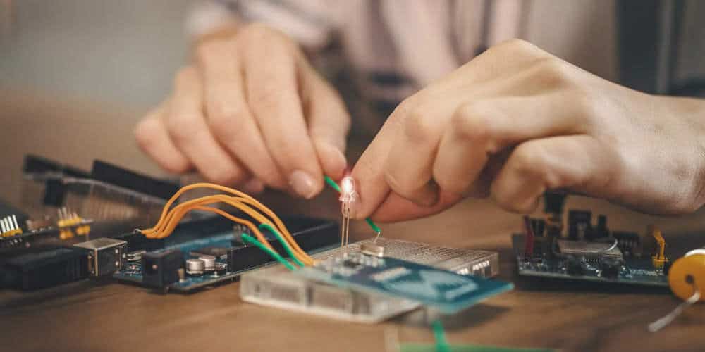
- Soldering Iron: This is a tool that is used to join components together by melting and fusing solder.
In addition to these tools, designers also use a range of other hardware tools such as power supplies, signal generators, and logic analyzers to test and troubleshoot circuits.
Overall, the tools and technologies used by printed circuit designers are essential to creating high-quality circuits that meet the needs of their clients. By using the right software and hardware tools, designers can create circuits that are reliable, efficient, and cost-effective.
Design Process
The design process of a printed circuit board (PCB) involves several stages, including schematic design, layout design, testing, and verification. Each stage is critical to ensure the final product functions as intended.
Schematic Design
The schematic design stage involves creating a visual representation of the circuit using a software tool. This stage is where the functionality of the circuit is defined, and the components that make up the circuit are selected. During this stage, it is important to consider factors such as power requirements, signal integrity, and component availability.
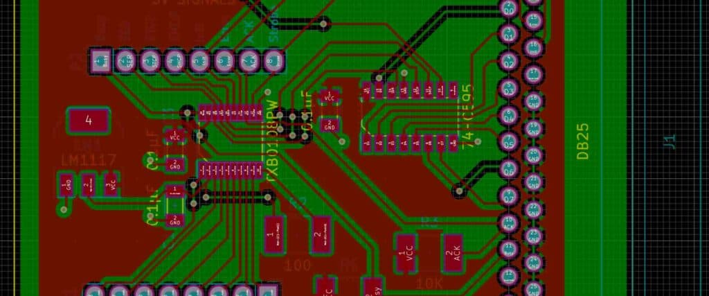
Layout Design
Once the schematic is complete, the layout design stage begins. This stage involves placing the components on the PCB and routing the connections between them. Careful consideration must be given to the placement of components to ensure that the final product meets size and performance requirements. Additionally, signal traces must be routed to minimize interference and noise.
Testing
After the layout design is complete, the PCB is manufactured and assembled. The testing stage involves verifying that the PCB functions as intended. This stage may involve the use of specialized equipment to measure performance and identify any issues.
Verification
Once testing is complete, the final stage is verification. This stage involves ensuring that the PCB meets all requirements and specifications. This includes verifying that the PCB is compatible with the intended application and that it meets regulatory requirements.
In conclusion, the design process of a printed circuit board involves several critical stages, including schematic design, layout design, testing, and verification. Each stage is essential to ensure that the final product functions as intended.
Collaboration and Communication
Collaboration and communication are crucial aspects of the printed circuit designer’s job. A successful designer must work effectively with their team and clients to ensure that the final product meets all requirements and specifications.
Teamwork
The design of a printed circuit board requires the collaboration of multiple professionals, including electrical engineers, mechanical engineers, and software engineers. The team must work together to ensure that the design meets all requirements and specifications. Effective communication is essential to ensure that everyone is on the same page and understands their role in the project.
To facilitate teamwork, designers often use project management software that allows team members to collaborate and communicate in real-time. This software can help to streamline the design process and ensure that everyone is working towards the same goal.
Client Interaction
Printed circuit designers must also communicate effectively with their clients. Clients may have specific requirements or specifications that must be met, and it is the designer’s responsibility to ensure that these requirements are incorporated into the design.
Effective client interaction requires clear communication and a deep understanding of the client’s needs. Designers must be able to explain technical concepts in a way that is easy for the client to understand. They must also be able to provide regular updates on the progress of the project and address any concerns or questions that the client may have.
In conclusion, collaboration and communication are essential skills for printed circuit designers. Effective teamwork and client interaction can help to ensure that the final product meets all requirements and specifications. By using project management software and effective communication strategies, designers can streamline the design process and deliver high-quality products to their clients.
Career Development
Education and Training
To become a printed circuit designer, you typically need a bachelor’s degree in electrical engineering, computer engineering, or a related field. Some employers may accept an associate’s degree or certificate program in electronics or computer-aided design (CAD).
In addition to formal education, on-the-job training is essential for career development. Printed circuit designers need to learn how to work with CAD software, read schematics, and understand the manufacturing process.
Certifications and Licenses
While not required, obtaining certifications can enhance a printed circuit designer’s career prospects. The most recognized certification in the industry is the Certified Interconnect Designer (CID) offered by the IPC Association. This certification demonstrates a designer’s proficiency in designing and manufacturing printed circuit boards.
Some states may require printed circuit designers to obtain a professional engineering license. This license typically requires a bachelor’s degree in engineering, passing the Fundamentals of Engineering (FE) exam, and gaining several years of work experience.
Professional Organizations
Joining a professional organization can provide printed circuit designers with access to industry resources, networking opportunities, and continuing education. The IPC Association and the Institute of Electrical and Electronics Engineers (IEEE) are two of the most prominent organizations in the field.
Membership in these organizations can also lead to career advancement opportunities, such as leadership positions or speaking engagements at industry conferences.
In summary, a printed circuit designer’s career development requires a combination of education, training, certifications, and involvement in professional organizations. By staying up-to-date with industry trends and advancements, a printed circuit designer can enhance their skillset and advance their career.
