Designing a Printed Circuit Board (PCB) can be a challenging task, especially for beginners. However, with the right tools and knowledge, it can be a rewarding experience. PCBs play a critical role in modern electronics, serving as the backbone of most electronic devices. They provide a platform for mounting and connecting electronic components, allowing for efficient and reliable operation.
To design a PCB, you need to have a good understanding of the circuit you want to build. This involves identifying the components you need, their specifications, and how they will be connected. Once you have a clear picture of the circuit, you can start designing the PCB layout. This involves placing the components on the board, routing the connections, and ensuring that the board meets all the necessary design rules and constraints.
In this article, we will explore the basics of designing a PCB. We will cover the tools and software needed, the steps involved in designing a PCB, and the common design rules and constraints. Whether you are a hobbyist or a professional, this article will provide you with the knowledge and skills needed to design your own PCBs.
Understanding PCB Design
What is PCB Design?
Printed Circuit Board (PCB) design is the process of creating a layout of electronic components on a board. It involves designing and arranging the components, traces, and vias to create a functional circuit that will perform as intended. The PCB design process is critical to the success of any electronic product, as it affects the performance, reliability, and cost of the final product.
Why is PCB Design Important?
PCB design is essential because it impacts the overall performance and functionality of the electronic device. A poorly designed PCB can cause signal interference, noise, and other issues that can negatively affect the performance of the device. Additionally, a poorly designed PCB can lead to manufacturing defects, which can result in costly rework and delays.
Basic PCB Design Process
The basic PCB design process involves several steps, including:
-
Schematic Design: This involves creating a schematic diagram of the electronic circuit, which shows the components and their connections.
-
Component Placement: This involves placing the components on the board in a way that optimizes performance, reduces noise, and minimizes the size of the board.
-
Routing: This involves creating the traces that connect the components on the board. The routing process must consider factors such as signal integrity, power distribution, and electromagnetic interference.
-
Design Rule Check (DRC): This involves running a DRC to check for errors in the design, such as short circuits, open circuits, and other problems.
-
Gerber Generation: This involves generating the Gerber files, which are used to manufacture the PCB.
In conclusion, PCB design is a critical process that impacts the performance, reliability, and cost of electronic products. Understanding the basics of PCB design is essential for creating functional and reliable electronic devices.
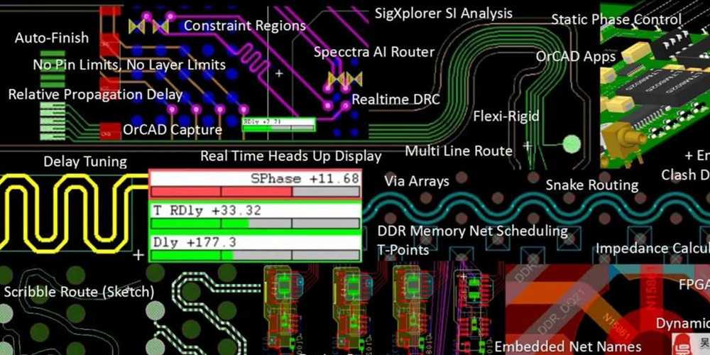
PCB Design Software
Popular PCB Design Software
There are many PCB design software options available on the market, each with its own unique features and benefits. Some of the most popular software options include:
- Altium Designer
- Eagle PCB Design
- KiCAD
- CircuitMaker
- OrCAD PCB Designer
Each of these software options has its own strengths and weaknesses, so it is important to carefully evaluate each one to determine which is the best fit for your specific needs.
Choosing the Right PCB Design Software
When selecting a PCB design software, there are several factors to consider:
- Ease of use: Look for software that is intuitive and easy to learn, especially if you are new to PCB design.
- Features: Consider the specific features you need, such as schematic capture, layout tools, and simulation capabilities.
- Compatibility: Make sure the software is compatible with the operating system you are using.
- Cost: PCB design software can range from free to thousands of dollars, so consider your budget when making a decision.
Ultimately, the right PCB design software will depend on your specific needs and preferences. Take the time to research and evaluate different options to find the one that is the best fit for you.
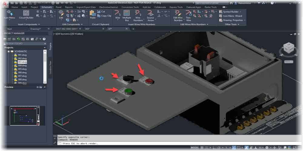
Creating Your PCB Layout
When it comes to designing a printed circuit board (PCB), creating the layout is a crucial step in the process. This section will cover the three main sub-sections of the layout process: Schematic Design, Component Placement, and Routing.
Schematic Design
The first step in creating your PCB layout is to create a schematic. This is a visual representation of the circuit you want to build. It shows the connections between components and their values.
When designing your schematic, it is important to keep it organized and easy to read. Use labels and symbols that are easy to understand. This will make it easier to move on to the next step of the layout process.
Component Placement
Once you have your schematic designed, the next step is to place your components on the board. This step is where you will decide where each component will go and how they will be arranged.
When placing your components, consider the size of each component and how they will fit on the board. It is also important to consider the connections between components and how they will be routed.
Routing
The final step in creating your PCB layout is routing. This is where you will connect the components on the board.
When routing, it is important to keep the traces as short as possible. This will help reduce noise and interference. You should also avoid crossing traces, as this can cause interference.
In conclusion, creating your PCB layout is an important step in the design process. By following the three sub-sections of Schematic Design, Component Placement, and Routing, you can create a well-organized and functional PCB.
PCB Manufacturing

When it comes to designing your PCB, you’ll eventually need to move on to the manufacturing process. This is where your design will be brought to life and turned into a physical circuit board. In this section, we’ll cover the basics of PCB manufacturing, including how to prepare your design for manufacturing and how to choose a PCB manufacturer.
Preparing Your Design for Manufacturing
Before you can send your design off to the manufacturer, there are a few things you need to do to ensure it’s ready for production. Here are some key steps to take:
-
Check your design for errors: Before you send your design off, make sure to double-check it for any errors or issues. This can include things like missing connections, incorrect footprints, or design rule violations.
-
Generate Gerber files: Gerber files are a set of files that describe your PCB design in a standardized format that manufacturers can use to produce your board. Most PCB design software will have an option to generate Gerber files automatically.
-
Choose your PCB specifications: This includes things like the number of layers, board thickness, copper weight, and more. Make sure to choose specifications that fit your design requirements and budget.
Choosing a PCB Manufacturer
Choosing the right PCB manufacturer is crucial to ensuring your design is produced correctly and on time. Here are some things to consider when selecting a manufacturer:
-
Experience and reputation: Look for a manufacturer with a proven track record of producing high-quality PCBs. Read reviews and ask for references to get a sense of their reputation in the industry.
-
Capabilities and equipment: Make sure the manufacturer has the capabilities and equipment to produce your design. This includes things like the number of layers they can produce, their minimum trace and space requirements, and their ability to produce complex designs.
-
Pricing and lead times: Compare pricing and lead times from multiple manufacturers to find one that fits your budget and timeline.
By following these steps, you can ensure your PCB design is ready for manufacturing and find a reliable manufacturer to produce it.
PCB Assembly
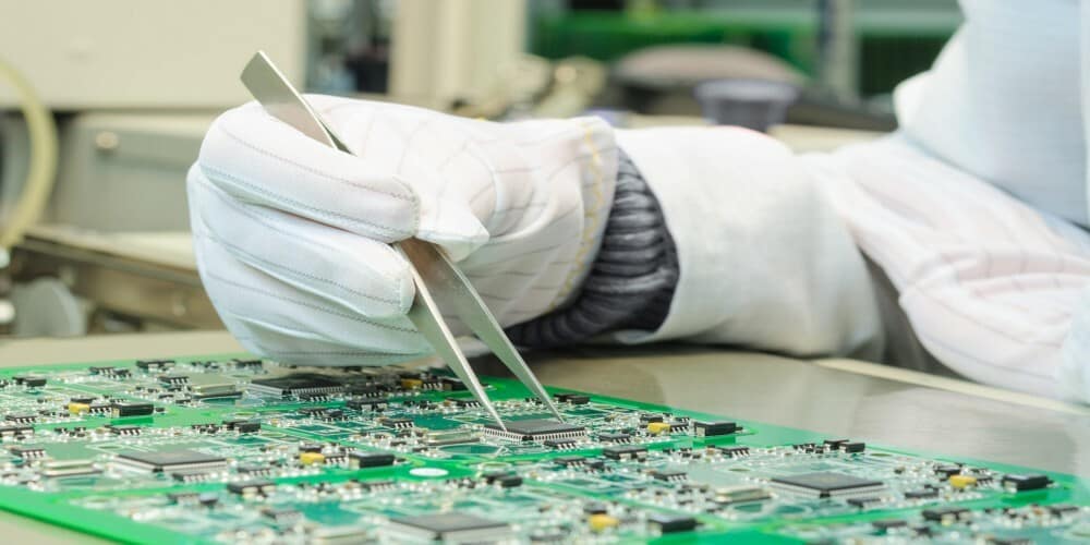
Preparing Your Design for Assembly
Before you begin the PCB assembly process, it’s important to ensure that your design is ready for assembly. This involves checking your design for errors, making sure that all components are correctly placed, and verifying that your design meets the requirements of your chosen PCB assembly service.
To prepare your design for assembly, you should follow these steps:
- Verify that all components are correctly placed and oriented
- Check for any design errors, including short circuits and open circuits
- Ensure that all components are properly labeled and identified
- Verify that your design meets the requirements of your chosen PCB assembly service
Choosing a PCB Assembly Service
When it comes to choosing a PCB assembly service, there are a few factors to consider. These include the service’s experience, reputation, pricing, and capabilities.
To choose the right PCB assembly service for your needs, you should consider the following:
- Experience: Look for a service that has experience assembling PCBs similar to yours
- Reputation: Check online reviews and ratings to ensure that the service has a good reputation
- Pricing: Compare pricing from multiple services to ensure that you’re getting a fair price
- Capabilities: Ensure that the service has the capabilities to handle your specific assembly requirements
By following these steps, you can ensure that your PCB assembly process goes smoothly and that your final product meets your requirements.
Testing and Troubleshooting Your PCB

PCB Testing
After completing the PCB design and manufacturing process, it is essential to test your board thoroughly before deploying it in a real-world application. PCB testing helps to identify any issues and ensure that the board functions as intended. Here are some testing methods to consider:
- Visual Inspection: This involves inspecting the board for any physical damage, incorrect components, or soldering issues.
- Continuity Testing: This verifies that there are no open or short circuits on the board.
- Functional Testing: This involves testing the board’s functionality using a test program or application to ensure that it performs as expected.
PCB Troubleshooting
Even with thorough testing, issues may arise after deploying the board. Here are some common PCB issues and troubleshooting methods:
- Power Issues: If the board is not receiving power or is experiencing voltage fluctuations, check the power supply and ensure that it meets the board’s requirements.
- Signal Integrity Issues: If the board is not functioning correctly, check for signal integrity issues such as noise, crosstalk, or impedance mismatches.
- Component Failure: If a component fails, replace it and test the board again.
In conclusion, testing and troubleshooting your PCB is a critical step in ensuring that it functions correctly. By following these methods, you can identify and resolve any issues before deploying the board in a real-world application.
