Switch-mode power supplies (SMPS) are essential components in modern electronic devices, providing efficient power conversion from AC to DC. SMPS PCB design is a critical aspect of the overall design process, as it directly affects the performance, reliability, and cost of the power supply.
A well-designed SMPS PCB can reduce the size and weight of the power supply while improving its efficiency, reliability, and electromagnetic compatibility (EMC) performance. However, designing an SMPS PCB requires careful consideration of various factors, including the topology, components, layout, and thermal management.
This article will provide an overview of SMPS PCB design, covering the key considerations and best practices for designing a high-performance, reliable, and cost-effective power supply. We will discuss the different SMPS topologies, component selection, layout guidelines, and thermal management techniques to help you design an optimized SMPS PCB for your application.
Overview of SMPS PCB Design
Switch Mode Power Supply (SMPS) is an electronic power supply that uses switching regulators to convert electrical power efficiently. The design of an SMPS PCB is critical to ensure the efficiency and reliability of the power supply.
An SMPS PCB design must consider several factors such as the type of power supply, the load requirements, the input voltage range, and the output voltage and current requirements. The design must also consider the thermal management, electromagnetic interference (EMI), and the safety regulations.
The primary objective of an SMPS PCB design is to minimize the power losses and maximize the efficiency of the power supply. This is achieved by selecting the appropriate components, such as the power switch, inductor, and capacitors, and optimizing the layout of the PCB.
The layout of the SMPS PCB is crucial to minimize the EMI and ensure proper thermal management. The placement of the components, the routing of the traces, and the use of ground planes and power planes are all critical to ensure the reliable operation of the power supply.
In summary, the design of an SMPS PCB is a complex process that requires careful consideration of several factors. The efficient and reliable operation of the power supply depends on the proper selection of components, the optimization of the layout, and compliance with safety regulations.
Key Considerations for SMPS PCB Design
When designing a Switched-Mode Power Supply (SMPS) PCB, there are several key considerations that must be taken into account to ensure optimal performance and reliability. Here are a few important factors to consider:
Component Selection
Choosing the right components is crucial for SMPS PCB design. Selecting high-quality components that can handle the expected power levels and are rated for the appropriate voltage and current levels is essential. It is also important to consider the operating temperature range and the expected lifespan of the components.
Layout and Routing
The layout and routing of the PCB can significantly impact the performance of the SMPS. The layout should be designed to minimize noise and interference, and to ensure that high-frequency signals are properly routed to minimize parasitic capacitance. The routing should be optimized to minimize the length of the traces and to ensure that there are no crossovers or loops that could cause interference.
Thermal Management
SMPS circuits generate heat, and it is important to design the PCB with adequate thermal management to prevent overheating and ensure reliable operation. This can be achieved through the use of heat sinks, thermal vias, and other cooling techniques.
EMI/EMC Compliance
SMPS circuits can generate significant electromagnetic interference (EMI) and electromagnetic compatibility (EMC) issues. It is important to design the PCB with EMI/EMC compliance in mind, including proper grounding, shielding, and filtering techniques.
Testing and Verification
Finally, it is important to thoroughly test and verify the SMPS PCB design to ensure that it meets all specifications and requirements. This can include functional testing, thermal testing, and EMI/EMC testing, among others.
Overall, designing an SMPS PCB requires careful consideration of a range of factors, from component selection to testing and verification. By taking these key considerations into account, designers can ensure optimal performance and reliability for their SMPS circuits.
Designing the Power Stage

The power stage of an SMPS (Switched-Mode Power Supply) is responsible for converting the input voltage to the desired output voltage. It is a crucial part of the SMPS and requires careful design to ensure its proper functioning. In this section, we will discuss the key considerations for designing the power stage of an SMPS.
Component Selection
The first step in designing the power stage is to select the appropriate components. The key components in the power stage include the power switch, the output diode, the output capacitor, and the inductor. The power switch and the output diode must be chosen based on their voltage and current ratings. The output capacitor must be selected based on its capacitance and voltage rating, while the inductor must be chosen based on its inductance and current rating.
Circuit Topology
The next step is to choose the circuit topology. The most common circuit topologies used in SMPS designs include the buck, boost, buck-boost, and flyback. The choice of circuit topology depends on the desired output voltage, current, and efficiency.
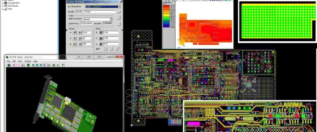
PCB Layout
The PCB layout is also an important consideration in designing the power stage. The layout must be designed to minimize the parasitic inductances and capacitances that can affect the performance of the SMPS. The power components should be placed close to each other to minimize the loop area and reduce the EMI (Electromagnetic Interference) emissions.
Control Circuitry
Finally, the control circuitry must be designed to ensure stable operation of the power stage. The control circuitry includes the feedback loop, which regulates the output voltage, and the gate driver circuit, which controls the power switch. The feedback loop must be designed to ensure stability and fast response, while the gate driver circuit must be designed to provide sufficient gate drive voltage and current to the power switch.
In summary, designing the power stage of an SMPS requires careful consideration of component selection, circuit topology, PCB layout, and control circuitry. By following these guidelines, designers can ensure the proper functioning of the power stage and achieve the desired performance of the SMPS.
Designing the Control Circuit
The control circuit is a crucial part of the SMPS PCB design. It is responsible for regulating the output voltage and current of the power supply. The design of the control circuit depends on the type of SMPS being used, such as flyback, forward, or push-pull.
One of the most important components of the control circuit is the feedback loop. The feedback loop continuously monitors the output voltage and adjusts the duty cycle of the switching transistor to maintain a constant output voltage. The feedback loop is typically implemented using an optocoupler or a voltage divider.
Another important component of the control circuit is the error amplifier. The error amplifier compares the output voltage to a reference voltage and generates an error signal that is fed into the feedback loop. The error amplifier is typically implemented using an operational amplifier.
The switching transistor is another critical component of the control circuit. The switching transistor is responsible for switching the input voltage on and off to create a high-frequency AC signal. The switching transistor must be able to handle high voltages and currents and must have a fast switching speed.
In addition to the components mentioned above, the control circuit may also include other components such as a soft-start circuit, overvoltage protection, and overcurrent protection. These additional components help to ensure that the power supply operates safely and reliably.
In conclusion, designing the control circuit for an SMPS is a complex process that requires careful consideration of the various components and their interactions. By following best practices and using high-quality components, it is possible to design a control circuit that provides stable and reliable power to the load.
Isolation and EMI Considerations
When designing an SMPS PCB, isolation and EMI considerations are crucial. The power supply must be isolated from the input source to ensure safety and prevent electrical shock. Isolation also helps to reduce noise and interference caused by ground loops, which can affect the performance of the power supply.
To achieve isolation, designers use transformers or optocouplers to provide a physical barrier between the input and output circuits. Transformers can provide galvanic isolation, which means there is no direct electrical connection between the primary and secondary windings. Optocouplers use a light-emitting diode (LED) and a photodetector to transmit signals across an isolation barrier.
In addition to isolation, designers must also consider electromagnetic interference (EMI). EMI can cause problems with other electronic devices and can even interfere with radio and television signals. To reduce EMI, designers use shielding, filtering, and grounding techniques.
Shielding involves enclosing the power supply in a metal case or using metal shields around sensitive components. Filtering uses capacitors and inductors to remove noise from the power supply output. Grounding techniques involve connecting the power supply to a common ground and using a low-impedance ground plane on the PCB.
Overall, isolation and EMI considerations are critical when designing an SMPS PCB. By using transformers or optocouplers for isolation and implementing shielding, filtering, and grounding techniques to reduce EMI, designers can create a safe and reliable power supply that meets the necessary regulatory standards.
Layout Considerations
The layout of an SMPS PCB design plays a crucial role in determining its performance, efficiency, and reliability. It is essential to pay attention to the following factors when designing the layout of an SMPS PCB.
Component Placement
The placement of components on the PCB is critical to achieving optimal performance. The placement of components should be such that the signal paths are as short as possible, and the loops formed by the signal and return paths are as small as possible. This helps to minimize noise and interference and reduce the risk of parasitic oscillations.
Ground Plane
The ground plane is an essential element in SMPS PCB design. A solid ground plane helps to reduce noise and interference and provides a low impedance path for the return currents. It is essential to ensure that the ground plane is continuous and that there are no breaks or gaps in it.
Trace Width and Spacing
The trace width and spacing are critical parameters that determine the current carrying capacity and impedance of the traces. It is essential to ensure that the trace widths are adequate to carry the required current without overheating and that the spacing between the traces is sufficient to prevent arcing.
Thermal Management
SMPS PCBs generate a lot of heat, and it is essential to ensure that the heat is dissipated efficiently to prevent overheating and damage to the components. It is essential to use thermal vias to transfer heat from the top layer to the bottom layer of the PCB and to use appropriate heatsinks and thermal pads to dissipate heat from the components.
EMI/EMC Considerations
SMPS PCBs generate a lot of electromagnetic interference (EMI) and can also be susceptible to electromagnetic compatibility (EMC) issues. It is important to ensure that the PCB layout is optimized to reduce EMI and that appropriate shielding is used to prevent EMC issues.
In summary, the layout of an SMPS PCB design is critical to achieving optimal performance, efficiency, and reliability. Component placement, ground plane, trace width and spacing, thermal management, and EMI/EMC considerations are all important factors that must be taken into account when designing the layout of an SMPS PCB.
Testing and Validation
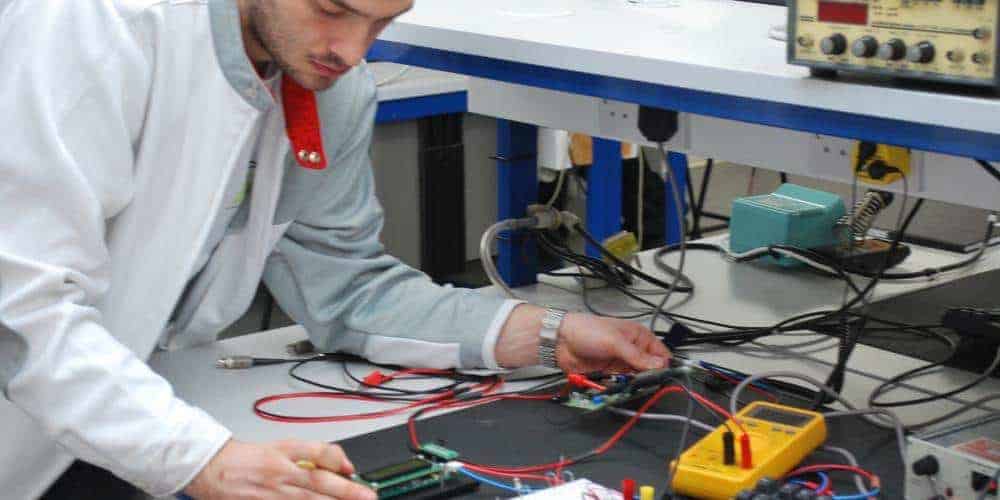
Once the SMPS PCB design has been completed, it is essential to test and validate the circuit to ensure that it meets the required specifications. Testing and validation are crucial steps in the design process as they help to identify any potential issues and ensure that the circuit is functioning correctly.
There are several different types of tests that can be performed on an SMPS PCB design, including functional testing, performance testing, and environmental testing. Functional testing involves testing the circuit’s various functions to ensure that they are working correctly. Performance testing involves measuring the circuit’s performance against a set of predefined specifications. Environmental testing involves subjecting the circuit to various environmental conditions to ensure that it can withstand these conditions.
One of the most critical aspects of testing and validation is ensuring that the circuit is safe to use. This involves testing the circuit’s isolation and ensuring that there are no hazardous voltages present. It is also essential to ensure that the circuit complies with relevant safety standards, such as UL or CE.
To perform these tests, specialized equipment is required, such as oscilloscopes, multimeters, and power supplies. It is also essential to have a good understanding of the circuit’s operation and the relevant specifications.
Once the testing and validation process is complete, any issues that have been identified can be addressed, and the circuit can be optimized for performance. This ensures that the circuit meets the required specifications and is safe to use.
In conclusion, testing and validation are essential steps in the SMPS PCB design process. They help to identify any potential issues and ensure that the circuit is functioning correctly and safely. By performing these tests, any issues can be addressed, and the circuit can be optimized for performance, ensuring that it meets the required specifications.
Conclusion

In conclusion, designing a Switched-Mode Power Supply (SMPS) PCB requires careful consideration of various factors. The design must be optimized for efficiency, stability, and reliability. The following key takeaways can be drawn from this article:
- The topology of the SMPS must be chosen based on the specific requirements of the application.
- The components used in the SMPS must be carefully selected to ensure that they are suitable for the application and can withstand the required operating conditions.
- The layout of the SMPS PCB must be optimized to minimize noise, ensure proper grounding, and minimize the length of high-current paths.
- The design must be thoroughly tested to ensure that it meets the required specifications and can operate reliably over the expected lifetime of the product.
Overall, designing an SMPS PCB can be a challenging task, but with careful planning and attention to detail, it is possible to create a high-performance and reliable power supply that meets the needs of the application. By following the guidelines outlined in this article, designers can ensure that their SMPS PCB designs are optimized for efficiency, stability, and reliability.
