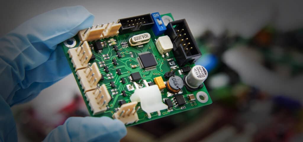
“Surface mount technology” (SMT) is a way to put together electronic parts by putting them directly on the surface of a printed circuit board (PCB). These parts are also known as “surface mount devices” (PCB). SMT is in high demand in the market because of its low cost and excellent quality efficiency. Moreover, SMT PCBs have become one of the most common and cost-effective methods of creating electrical circuits in recent years.
This article will explain what they are, why businesses use them, and what you should check out for if you plan to use them.
What Are SMT PCBs?
Understanding SMT PCB is not as simple as one may think it is. However, as the name suggests, the method of the PCB assembly process operates by putting components on a blank PCB. When building complicated PCBs, the SMT printer can generally accomplish this automatically while taking specific design directions. The accuracy that this technology gives is what makes it so significant. Prior to SMT, the ordinary PCB could only be so small until it became too difficult to handle. Currently, the SMT method allows PCB to be considerably smaller.
Unlike previously created PCBs, this is typically mechanized, saving everyone time and money.
In SMT assembly, parts aren’t put into holes; instead, they are soldered directly onto the board using reflow soldering.
How Does Surface Mount Technology Work?
Surface-mounted transistors, diodes, capacitors, and other parts are put on printed circuit boards (PCB assembly) using pick-and-place machines. These machines take part out of its storage container and put it on the PCB.
Sometimes surface mounting components come pre-applied with solder paste. You don’t need to use any extra paste to put these parts directly on the PCB. The components are then soldered together to make connections. Typically, soldering is achieved by placing a hot soldering iron on top of the component, melting the solder, and connecting it to the PCB.
Usually, a small piece of tape is put on the bottom of each SMT component to keep it in place while it is being stored, moved, or put together. This also prevents components from slipping off the PCB during construction (especially when using pick-and-place machines). The tape is removed before soldering.
SMT Assembly Process
The three phases of the SMT assembly process include printing solder paste, placing components, and reflow soldering. Due to the needs of the SMT production process, however, the following outline goes into more detail about these phases:
1. Preparation of SMC and PCB
Initial steps include selecting the SMCs and PCB. Solder pads are typically flat, free of holes, copper pads that are generally silver, tin-lead, or gold plated. Solder pads protect the pins of components such as transistors and semiconductors.
The stencil is another important tool used to create a fixed location for the next step of the process, which is printing the solder paste, depending on where the solder pads are already placed on the PCB. These materials and any others that will be used in the manufacturing process must be carefully checked for flaws.
2. The Solder Paste Printing
The solder paste application is an important stage in the SMT process. At this stage, the solder paste is put on at an angle of 45° to 60° with the help of a squeegee, which is a tool used to clean printing plates. To make solder paste, you mix together metal solder powder and flux, which is like glue. The flux acts as a temporary adhesive to bind the surface mount components in place while also cleaning contaminants and oxidation from the soldering surfaces.
To connect the SMC to the solder joints on the PCB, solder paste is also used. It is very important that each pad has the right amount of paste on it. If not, when the solder melts in the reflow oven, it won’t connect to anything. Reflow ovens are electrical heating devices used in surface mount technology (SMT) to attach electronic parts to printed circuit boards (PCBs).
3. SMC Placement
It is now time to install electrical components into the PCB. Manufacturers do this with a machine called a “pick and place” machine. The machine carefully puts the SMCs on the board. The PCB is ready for reflow soldering once the mounting process is done.
4. Soldering Reflow Process
When the SMCs are in place, the PCB is sent into the reflow soldering oven, where it passes through the following stages:
In the first part of the oven, called the “preheat zone,” the temperature of the board and all of its parts are slowly raised. The temperature goes up by 1.0°C to 2.0°C per second until it’s between 140°C and 160°C.
Soak zone: The board will stay at a temperature between 140°C and 160°C for 60–90 seconds.
The boards next enter the reflow zone, where the temperature is ramped up at 1.0°C-2.0°C per second to a maximum of 210°C-230°C to melt the tin in the solder paste, fusing the component leads to the PCB pads. The surface tension of the molten solder keeps the components in place while this is happening.
Cooling zone: this is the final part that ensures solder freezes upon exiting the heating zone to prevent linkage problems.
If the printed circuit board has two sides, repeat these steps. To keep the SMCs in place, you can use solder paste or glue.
5. Inspection and cleaning
The board is then inspected for flaws and cleaned after soldering is complete. After soldering, the PCB cleaning step is critical. Following the completion of the cleaning procedure, the operators inspect the PCB for defects. Before storing it, they must make any necessary repairs or reconstructions.

Advantages of SMT
• Reduced manufacturing costs
Because there is no need for a pre-drilled PCB, not only does the process take less time than THT, but it also costs less because fewer steps are appropriate. SMT components are up to 10 times quicker to position than THT components.
• A more dependable solder
Better results can be expected when using SMD soldering paste. Most of the time, a machine puts the components into the SMT soldering paste, a stencil is used to cover the spaces that are left open, and the PCB is heated to reflow the paste. It has been shown that this type of soldering is more reliable and can handle stress and vibration better.
• More compact PCBs and devices
When there are parts on both sides of the board, the density goes up. This results in smaller PCBs.
• Reduced resistance and inductance in the connection
Reduces radiated emission by using smaller components and a smaller connection area.
· Devices for SMT
Surface mount components vary from their leaded equivalents. Direct soldering of SMT components to a circuit board eliminates the need for cables.
Their leads do not pass through holes in the board, as one might expect from a traditional leaded component. There are various package styles for various types of components. Passive components, transistors and diodes, and integrated circuits are the three main types of SMT components, and they include:
• Passive SMDs
There are many different packages available for passive SMDs. However, the vast majority of passive SMDs are either SMT resistors or SMT capacitors, both of which have fairly standardized package sizes. Other components, such as coils, crystals, and others, have more specific requirements and thus require their own packages.
• Package sizes for resistors and capacitors vary
These have the following designations: 1812, 1206, 0805, 0603, 0402, and 0201. In hundreds of an inch, the measurements are given. In other words, 1206 is 12 x 6 hundredths of an inch in size. There was an early preference for larger sizes, such as 1812 and 1206. As a result of the necessity for smaller components, they are hardly ever in use today. However, they may be useful in situations requiring higher power levels or if other factors necessitate a bigger size.
At both ends of the package, there are metalized spots that make connections to the printed circuit board.
A lot of the time, SMT transistors and diodes come in tiny plastic containers. The leads stick out of the package and are easily bent to touch the board, and they always use three leads. This makes it simple to determine which way the device must be turned.
· Integrated circuits
Packages for integrated circuits come in a range of sizes. How much connectivity is needed will determine which package to choose. Many devices, such as basic logic chips, may only need 14 or 16 pins, but others, such as VLSI processors and accompanying circuits, may need 200 or more. Because of the vast range of needs, a variety of packages are available.
Smaller chips can use SOIC (Small Outline Integrated Circuit) packaging. These are essentially SMT versions of the well-known DIL (Dual In Line) packaging used for the well-known 74 series logic chips. There are even smaller variations, such as TSOP (Thin Small Outline Package) and SSOP (Shrink Small Outline Package).
VLSI chips need different methods. It is common to practice using a four-sided flat pack. This features a square or rectangular footprint with pins on all four sides. When the pins come out of the package, they are ready to bend again into a gull-wing shape, so they will fit the board. The distance between the pins depends on how many pins there are. It might be as near as 20 thousandths of an inch for certain chips. Because the pins on these chips are easily bendable, you have to be very careful when shipping and handling them.
There are further bundle options. Many applications make use of a BGA (Ball Grid Array). The connectors are located under the package rather than on the side. The solder balls on the connecting pads melt during the soldering process, forming a good connection with the board and mechanically connecting it. Because the entire underside of the package can be used, the pitch of the connections is broader and much more efficient.
Some ICs also use a smaller version of the BGA known as the micro BGA. It is, as the name implies, a scaled-down version of the BGA.
Because of the widespread use of surface mount technology, a wide range of components is now accessible. The number of components available in surface mount packages vastly outnumbers those in classic leaded forms. This is solely due to high demand.
But common basic parts like transistors and different kinds of logic and analog ICs, like operational amplifiers, are often available in both surface mount and normal leaded versions.
What is the difference between SMT vs. SMD?
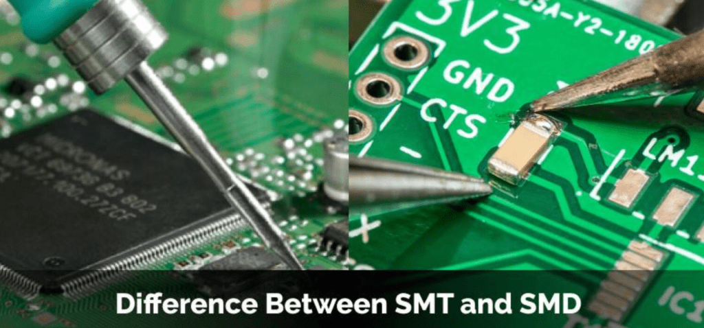
People often mix up the terms SMT and SMD, and the terms are often used in the same way. Indeed, any technology and its physical components may become closely interwoven, causing uncertainty. Both SMT and SMD fall into this category. This is why understanding the distinction between an SMT assembly and individual SMD components is critical.
In a nutshell, the method of SMT PCB technology is, when SMD is the technology’s device. SMT refers to the process of directly putting and soldering electrical components on a PCB. Surface mount devices, or SMDs, are another name for these components. The purpose is to place them on a printed circuit board (PCB).
SMD PCB provide quicker device production, more flexibility, and lower costs without losing functionality. Because smaller components allow for more circuits on a smaller board area, they offer more functionality. SMD’s main characteristic is its miniaturization.
SMT PCB and SMD PCB work together to offer consumers PCBs that are quicker, more energy-efficient, and more reliable.
Conclusion
SMT’s significant benefits are its smaller size, faster manufacturing, and lighter weight, which leads to considerably simpler electronic circuitry design and manufacture, which is particularly important in printed circuit board assembly and complicated circuits. Throughout the electronics manufacturing business, this increased degree of automation has saved time and money. Thus, despite the constant development of new technologies, SMT has undoubtedly maintained its significance.
