The TDA1524A preamplifier PCB layout is a critical component of any high-quality audio system. This preamplifier is designed to provide exceptional sound quality, with low distortion and high signal-to-noise ratios. The PCB layout is a critical aspect of the design, as it determines the performance of the preamplifier.
One of the key features of the TDA1524A preamplifier is its ability to adjust the frequency response of the audio signal. This allows the preamplifier to compensate for deficiencies in the audio system, such as speaker or room acoustics. The PCB layout is designed to ensure that this feature operates correctly, with minimal noise and distortion.
Overall, the TDA1524A preamplifier PCB layout is an essential aspect of any high-quality audio system. With its ability to adjust the frequency response and low distortion, this preamplifier is an excellent choice for audiophiles looking to get the most out of their audio system.
TDA1524A Preamplifier PCB Layout Design
Overview
The TDA1524A is a stereo preamplifier integrated circuit (IC) that is commonly used in high-end audio systems. The PCB layout for the TDA1524A preamplifier is critical to ensure optimal performance and minimize noise and interference.
Components
The TDA1524A preamplifier requires a few key components, including resistors, capacitors, and an optional potentiometer. The values of these components will depend on the specific design and application of the preamplifier.
Schematic Diagram
The schematic diagram for the TDA1524A preamplifier provides a visual representation of the electrical connections between the various components. It is important to carefully review and understand the schematic diagram before designing the PCB layout.
Layout Design
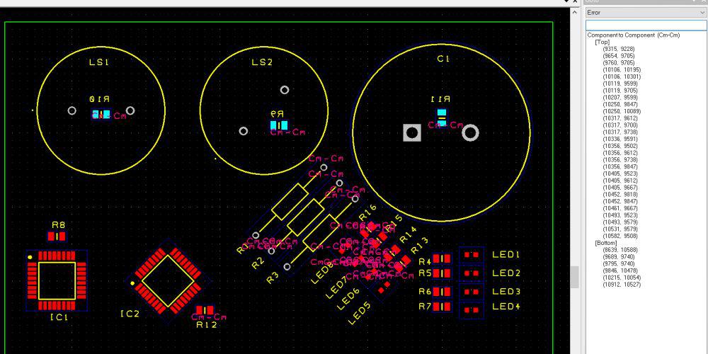
The PCB layout for the TDA1524A preamplifier should be designed with careful consideration to minimize noise and interference. This can be achieved by keeping the signal traces as short as possible, using a ground plane, and separating the power supply traces from the signal traces.
It is also important to ensure proper component placement on the PCB to minimize the length of the signal traces. This can be achieved by grouping components together based on their function and arranging them in a logical and efficient manner.
Overall, the TDA1524A preamplifier PCB layout design should prioritize signal integrity and noise reduction to ensure optimal performance in high-end audio systems.
PCB Fabrication

PCB Design Software
The first step in creating a PCB layout for the TDA1524A preamplifier is to use a PCB design software. There are several software options available, including Eagle, KiCad, and Altium Designer. These software programs allow you to create a schematic of your circuit, then convert it into a PCB layout. You can also choose the size and shape of your PCB, add components, and create a bill of materials.
PCB Manufacturing Process
Once you have created your PCB layout, it’s time to manufacture the PCB. There are several steps involved in this process, including printing the layout onto the copper-clad board, etching the board to remove unwanted copper, drilling holes for components, and adding a solder mask and silkscreen.
There are several methods for manufacturing PCBs, including toner transfer, photoengraving, and direct imaging. Each method has its pros and cons, and the best method for you will depend on your budget, skill level, and the complexity of your PCB layout.
PCB Assembly Process
After you have manufactured your PCB, it’s time to assemble the components. This process involves placing components onto the PCB, then soldering them in place. There are several methods for assembling PCBs, including hand soldering, reflow soldering, and wave soldering.
Hand soldering is the most common method for small-scale PCB assembly, while reflow soldering and wave soldering are more suitable for large-scale production. It’s important to follow proper soldering techniques to ensure a reliable and long-lasting connection between your components and your PCB.
In conclusion, creating a PCB layout for the TDA1524A preamplifier involves using a PCB design software, manufacturing the PCB using one of several methods, and assembling the components using proper soldering techniques. With the right tools and techniques, you can create a high-quality PCB that will provide reliable performance for years to come.
Testing and Troubleshooting

Testing Procedures
When testing the TDA1524A preamplifier PCB layout, it is important to follow a set of procedures to ensure accurate results. Here are some steps to follow:
- Connect the preamplifier to an audio source and an amplifier.
- Turn on the audio source and the amplifier.
- Set the volume to the lowest level.
- Gradually increase the volume level and listen for any distortion or noise.
- Use a multimeter to measure the voltage at various points on the PCB layout to ensure proper voltage levels.
- Check the connections and solder joints for any loose or cold joints.
Troubleshooting Tips
If you encounter any issues with the TDA1524A preamplifier PCB layout, here are some troubleshooting tips:
- Check the power supply voltage to ensure it is within the recommended range.
- Check the input and output connections for any loose or cold joints.
- Check the solder joints for any defects or cracks.
- Check the components for any damage or incorrect values.
- Use a signal tracer to trace the signal path and identify any issues.
- Refer to the datasheet and schematic diagram to identify any potential issues.
By following these testing procedures and troubleshooting tips, you can ensure that your TDA1524A preamplifier PCB layout is functioning properly and producing high-quality audio output.
