Watching a skilled and experienced cook prepare a rare dish can be so entertaining and fascinating. Seeing them combine various ingredients, seasonings, and sauces to create a gastronomic masterpiece is one event to tick off one’s bucket list, so to speak. It would even be more impressive if one was restricted to, say, just four condiments, being a mix of various sauces, ingredients, and condiments. That would probably be one to watch, from start to finish.
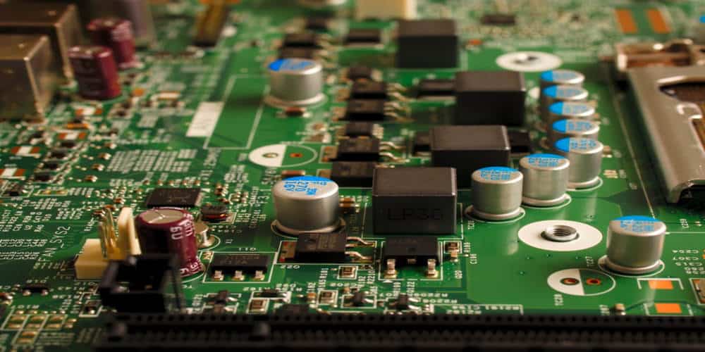
A miracle of this sort happens in the electronics manufacturing industry, in the PCB manufacturing sector. PCB (printed circuit board) designers create a unique type of board that has just four layers in one setup. This allows for greater power and higher potential to add features to electronics like laptops and smart electronics. The PCB sub-sector is much of an unknown entity, and this is mainly because their products are hidden while they do their jobs.
There are many reasons why circuit board engineers design boards with four layers. They accrue many benefits and are very economical. They are also a great way to save some costs from the manufacturing process which is why many consumers consider them.
However, there is a catch.
Designing with four layers on a PCB introduces some unique challenges. It can be tough trying to meet specific requirements such as satisfying the routing and signal integrity requirements of the board. It can also be a bit difficult to develop a restrictive design that meets design criteria such as cost, size, electrical performance, and manufacturability (this begins with correctly configuring the layer stack-up).
This piece highlights some recommendations and information about the 4-layer PCB design.

What Is a 4-Layer PCB Design?
Printed circuit boards are vital components of electronic circuits and can be single or multi-layered. While simple circuits use one layer and two layers, complex circuits use four to six PCBs at once. This implies that the higher the complexity, the higher the number of PCBs used. PCBs not only differ in layers but also in complexity.
PCBs can either be flexible, rigid, or rigid-flex. Likewise, they can also be single-sided, double-sided, or multi-sided. Rigid PCBs are solid, and they cannot be modified into any other shape after they are made. They can also appear multilayered.
Rigid PCBs are mainly used in several circuits as they are cost-effective and much more durable. Seeing that they are very dense and of top quality, they are used for numerous applications in various electronic devices. It’s no wonder they are highly demanded, and this demand is increasing by the day when compared to flexible PCBs.
A 4-layer PCB is a type of printed circuit board used in the electronic industry that features double-blind via and internal layers. This type of PCB possesses 4 layers that channel electrical signals. The layers comprise a top layer, two inner layers (VCC and GND), and a bottom layer. The outward layers are the top and bottom layers, and the two inner layers serve as the core. These layers work as signal routing or power planes.
4-layer PCBs support a highly complex circuit simply because each layer is made from copper. These four layers are joined together with fiberglass etched in between them. This is what makes them durable and rugged.
It is important to know the type and complexity of your circuit as it will determine the type of PCB you will need. PCBs are manufactured in steps and with PCB design software, and this will be addressed later.
Why Should You Choose a 4-Layer PCB Design?
Below are reasons why you should opt for a 4-layer PCB over other types of PCB:
- 4-layer PCBs are lightweight and smaller in size when compared to 2-layer PCBs. This is because the increased number of layers allows for a wider scope when addressing compact routing strategies. This also allows them to be used in small electronic applications such as smartwatches, tablets, smartphones, and laptops.
- 4-layer PCBs prove to be of higher quality than 2-layer PCBs. This is due to the improved noise reduction and signal integrity.
- The higher the number of layers a PCB possesses, the higher the power capability of the device the PCB is used. 4-layer PCBs are more powerful (can take on more electrical power requirements) than 2-layer PCBs.
- Circuit complexity is done only because of the constant need of electronic manufacturers to add new features to products. The higher the complexity of the circuit, the easier it is for manufacturers to add new features. Hence, 4-layer PCBs are more suitable and demanded by electronic manufacturers than 2-layer PCBs.
- The higher the number of layers a PCB possesses, the higher its mechanical strength. This is because the more layers a PCB has allows for less geometrical distortions such as warps.
- A higher number of layers in a PCB aids a more distributed and balanced copper level in the stack-up. This in turn enhances PCB performance.
While costs and lead times are usually slightly higher for 4-layer PCB designs, the benefits far outweigh the drawbacks. Benefits such as compact design possibilities and high-speed operation are just some of the many advantages that are currently ramping up the demand, usage, and applications of 4-layer PCBs when compared to 2-layer PCBs.
Steps to Follow for a 4-Layer PCB Design

As with anything that will be designed, there is a process to be followed to ensure a good output, and 4-layer PCBs are not left out. Many dependable and solid tools can be used when there is a need to design 4-layer PCBs. EasyEDA is a good choice, and others are OrCAD PCB Designer, Allegro, Altium, Mentor PADS, and PCB Design and Analysis Tools.
The steps to design 4-layer PCBs are listed and explained below:
1. Sketch the schematics
To begin a 4-layer PCB design, one needs to sketch the schematics. The schematics refer to the design of the board at the electrical level, which is determined by the board’s purpose, function, and the device it will be used in. The schematic becomes the blueprint for the design, and it would be needed throughout the design process. When sketching the schematic, some details need to be included, and they are listed below:
- The components to be used in layer stack-up design.
- The relationship between the component groups.
- The connection between the components
You will need to provide the correct dimensions for the design and verify it. Also note that at this point, schematics cannot be referred to as mechanical representations.
2. Create your PCB layout
Once you have your sketch, you are ready to create the PCB layout using a schematic capture tool. This is where the process of the board’s operation and where each component will be placed is determined.
This entails following standards and all criteria as dictated by the IPC, the association for electronics and PCB manufacturing. It is advisable to converse with a PCB layout provider who is very familiar with these standards. This will help you avoid delays and revisions.
3. Place the components and arrange them properly
Placing components is the next step, and like the previous step, it involves having an industry professional at hand. Also, it will be important to arrange the components according to the client’s specifications. For instance, the client might indicate in the data sheet that certain components should not be placed close to each other for certain reasons.
Furthermore, while designing, note that placing components of the same function near each other will make your design look as clean as possible.
4. Select auto or manual routing for the components
Next is to select the routing and the routing priority. You should opt for auto routing as it will give you the best routing chance for the circuit while highlighting the routing priority.
5. Conduct a final review and assessment of all the components
The last step is to conduct a review, which will include testing and assessment. This is important as it is the only way to ensure that the PCB will meet all the client’s needs during its use. If it does not pass testing, it needs to go back to the drawing board and adjust.
Final Words
With advancements in technology growing each day, there is so much demand for the quality and quantity of multilayer PCBs. This is why the PCB manufacturing process is done under optimal conditions and is strictly supervised. Therefore maintaining the quality of the boards and safety for users is of topmost priority. Do not be deceived, however, making PCBs can be lots of fun and rewarding, and 4-layer PCBs are even more fun, as many PCB designers would affirm.
If you are looking to get new and basic information and knowledge for your prototype circuit on your PCB, this article is your best hope. You will surely find it easier to approach your PCB design projects and finish them as soon as you can.
Also, if you need help with your next PCB order, we are here to fulfill that need. Contact us and let us get started with your order. See you soon!
