Altium Designer 4 layer PCB is a popular software tool used in the design and development of printed circuit boards. It offers a comprehensive set of features for designing and testing PCBs, making it a valuable asset for engineers and designers.
With its user-friendly interface and powerful design tools, Altium Designer 4 layer PCB enables users to create complex designs with ease. The software allows for the creation of multi-layered PCBs, which can be used in a variety of applications, including consumer electronics, medical devices, and industrial equipment.
Whether you are a novice or an experienced designer, Altium Designer 4 layer PCB offers a range of tools and features that can help you create high-quality, reliable PCBs. From schematic capture to layout design and testing, the software provides a complete solution for all your PCB design needs.
Basics of Altium Designer
What is Altium Designer?
Altium Designer is a powerful and intuitive PCB design software that is used by engineers and designers to create and develop printed circuit boards. It is a comprehensive design tool that includes schematic capture, PCB layout, and design verification features, all in one package.
Why use Altium Designer?
Altium Designer is widely regarded as one of the best PCB design software tools available on the market today. It offers a wide range of features and capabilities that make it an ideal choice for both beginners and experienced designers. Some of the key benefits of using Altium Designer include:
- Comprehensive design tool: Altium Designer offers a complete suite of design tools that can help you create and develop complex PCB designs quickly and easily.
- User-friendly interface: The software’s intuitive and user-friendly interface makes it easy to use for both beginners and experienced designers.
- Powerful design features: Altium Designer offers a wide range of powerful design features, including schematic capture, PCB layout, design verification, and more.
- Advanced routing capabilities: The software’s advanced routing capabilities allow you to create complex PCB layouts with ease.
- Robust design rule checking: Altium Designer’s design rule checking feature ensures that your designs meet industry standards and are error-free.
Key features of Altium Designer
Altium Designer includes a wide range of features and capabilities that make it an ideal choice for PCB design. Some of the key features of Altium Designer include:
- Schematic capture: Altium Designer’s schematic capture feature allows you to create and edit schematics quickly and easily.
- PCB layout: The software’s PCB layout feature allows you to create complex PCB layouts with ease.
- Design rule checking: Altium Designer’s design rule checking feature ensures that your designs meet industry standards and are error-free.
- 3D visualization: The software’s 3D visualization feature allows you to view your designs in 3D, giving you a better understanding of how your PCB will look and function.
- BOM management: Altium Designer’s BOM management feature allows you to manage your bill of materials (BOM) easily and efficiently.
- Integrated libraries: The software includes a wide range of integrated libraries, including schematic symbols, PCB footprints, and 3D models.
In conclusion, Altium Designer is a powerful and intuitive PCB design software that offers a wide range of features and capabilities. It is an ideal choice for both beginners and experienced designers, thanks to its user-friendly interface, advanced routing capabilities, and robust design rule checking feature.
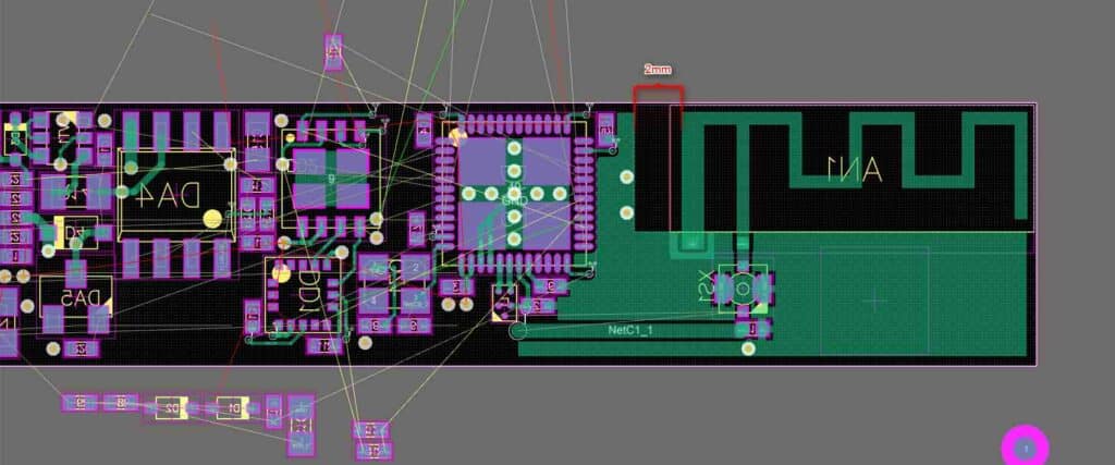
Designing a 4 Layer PCB

Understanding 4 Layer PCBs
A 4 layer PCB is a printed circuit board that consists of four layers of conductive material separated by insulating layers. This type of PCB is commonly used in electronic devices that require a high density of components and a complex circuit design. The four layers of a 4 layer PCB include two signal layers, a power plane, and a ground plane. The signal layers are used for routing the signals between the components while the power and ground planes provide a stable power supply and ground connection to the components.
Creating a new PCB project
To create a new PCB project in Altium Designer, go to the File menu and select New > PCB Project. Give your project a name and save it to a location on your computer.
Setting up the PCB design rules
Before starting the design, it is important to set up the PCB design rules. This includes defining the layer stack, trace widths, spacing, and clearance rules. To set up the design rules in Altium Designer, go to the Design menu and select Rules.
Importing schematic into PCB layout
Once the design rules are set up, the next step is to import the schematic into the PCB layout. To do this in Altium Designer, go to the Design menu and select Import Changes from Schematic. This will bring up a window where you can select the schematic file and import it into the PCB layout.
Placing components on the PCB layout
After importing the schematic, the next step is to place the components on the PCB layout. To do this in Altium Designer, go to the Place menu and select Component. This will bring up a window where you can select the component from the library and place it on the PCB layout.
Routing traces on the PCB layout
Once the components are placed, the next step is to route the traces on the PCB layout. To do this in Altium Designer, go to the Route menu and select Interactive Routing. This will allow you to route the traces by clicking on the pins of the components and dragging the trace to the desired location.
Adding vias and through-holes
To connect the different layers of the PCB, vias and through-holes are used. To add vias and through-holes in Altium Designer, go to the Place menu and select Via or Hole. This will allow you to add the via or hole to the desired location on the PCB layout.
Finalizing the design
Once the design is complete, it is important to check for any errors or design rule violations. To do this in Altium Designer, go to the Design menu and select Design Rules Check. This will check the design for any errors or violations and provide a report. Once the design is error-free, it can be sent for fabrication.
In summary, designing a 4 layer PCB involves understanding the layer stack and design rules, importing the schematic into the PCB layout, placing the components, routing the traces, adding vias and through-holes, and finalizing the design. By following these steps, you can create a high-quality 4 layer PCB using Altium Designer.
Advanced Techniques

Using design rules to optimize the design
Design rules are a set of parameters that define the minimum and maximum values for various aspects of the design, such as trace width, clearance, and via size. By using design rules to optimize the design, you can ensure that the PCB meets the required specifications and is manufacturable.
Adding copper pours to the PCB layout
Copper pours are large areas of copper that are placed on the PCB to provide a low-impedance ground or power plane. They can also be used to reduce the amount of noise in the signal traces. By adding copper pours to the PCB layout, you can improve the signal integrity and reduce the electromagnetic interference (EMI) in the design.
Creating custom footprints
A footprint is a physical representation of a component on the PCB. Creating custom footprints allows you to ensure that the component fits perfectly on the PCB and is placed in the correct location. By creating custom footprints, you can also ensure that the component has the required electrical characteristics and is compatible with the rest of the design.
Using differential pairs and controlled impedance
Differential pairs are a pair of traces that carry a differential signal. Controlled impedance is the characteristic impedance of a trace that is maintained throughout the length of the trace. By using differential pairs and controlled impedance, you can ensure that the signal is transmitted with minimal distortion and noise.
Design for Manufacturing (DFM) considerations
Design for Manufacturing (DFM) is a set of guidelines that ensure that the PCB can be manufactured easily and cost-effectively. DFM considerations include things like panelization, fiducials, and solder mask expansion. By considering DFM during the design phase, you can reduce the cost and time required for manufacturing.
In summary, Altium Designer provides advanced techniques for optimizing the PCB design. By using design rules, adding copper pours, creating custom footprints, using differential pairs and controlled impedance, and considering DFM, you can ensure that your PCB meets the required specifications and is manufacturable.
Conclusion
In conclusion, Altium Designer is a powerful tool for designing 4 layer PCBs. Its intuitive user interface and extensive library of components make it easy to create complex designs quickly and efficiently.
One of the key benefits of using Altium Designer is its ability to provide a complete design solution, from schematic capture to PCB layout and manufacturing output. This streamlines the design process and minimizes the risk of errors or inconsistencies.
Altium Designer also offers a range of advanced features, such as differential pair routing, high-speed design rules, and 3D visualization, which make it suitable for designing high-performance PCBs for a variety of applications.
Overall, Altium Designer is a reliable and user-friendly tool for designing 4 layer PCBs. Its comprehensive feature set, coupled with its ease of use, makes it a popular choice for both novice and experienced designers alike.
