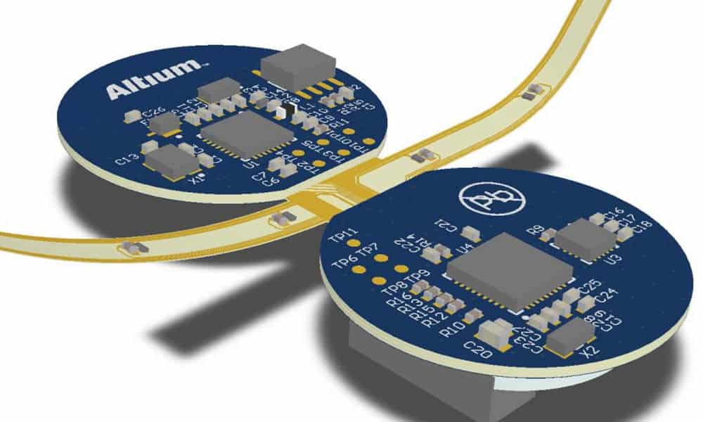
Altium Multilayer PCB design is an advanced technology that is becoming increasingly popular in the electronics industry. This design allows for multiple layers of printed circuit boards to be stacked on top of each other, providing more space for components and reducing the overall size of the board. The process of designing and manufacturing these boards can be complex, but the benefits are undeniable.
One of the key advantages of using Altium Multilayer PCB design is the ability to create smaller and more compact devices. With traditional single-layer PCBs, designers are limited in the amount of space available to place components. However, with multilayer designs, components can be placed on multiple layers, allowing for a more efficient use of space. This can be particularly useful in devices such as smartphones, where space is at a premium.
Basics of Altium Multilayer PCB Design
Altium is a popular software tool that engineers use to design multilayer printed circuit boards (PCBs). Multilayer PCBs are widely used in modern electronics due to their ability to support complex circuit designs and provide better signal quality. Here are some basics of Altium multilayer PCB design:
-
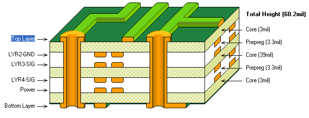
Layer stackup: The first step in Altium multilayer PCB design is to define the layer stackup. This involves selecting the number of layers, their thickness, and the material used. Altium provides a user-friendly interface to define the layer stackup, and engineers can choose from a wide range of materials to optimize the performance of their PCBs.
-
Component placement: Once the layer stackup is defined, engineers can start placing components on the PCB. Altium provides a powerful component placement tool that allows engineers to place components manually or automatically. Engineers can also use the “Design Rules” feature to ensure that components are placed correctly and to avoid design errors.
-
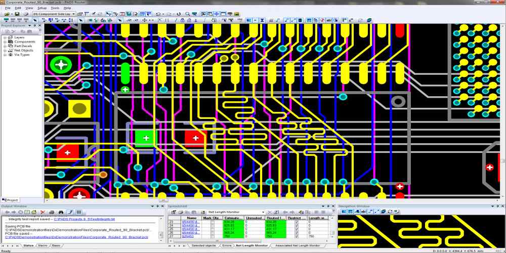
Routing: After component placement, the next step is to route the traces. Altium provides a user-friendly interface to route the traces, and engineers can choose from a wide range of routing options to optimize the performance of their PCBs. Altium also provides a “Design Rules” feature to ensure that the routing is done correctly and to avoid design errors.
-
Signal integrity: Altium provides a range of tools to optimize the signal integrity of multilayer PCBs. Engineers can use the “Signal Integrity” feature to analyze the signal quality of their PCBs and to optimize the routing to minimize signal loss and noise.
-
Manufacturing: Once the design is complete, engineers can generate manufacturing files using Altium. Altium provides a range of file formats to support different manufacturing processes, and engineers can choose the appropriate format based on their requirements.
In conclusion, Altium is a powerful tool for designing multilayer PCBs. Its user-friendly interface and powerful features make it a popular choice among engineers. By following the basics of Altium multilayer PCB design, engineers can design high-performance PCBs that meet their requirements.
Design Considerations for Altium Multilayer PCBs

When designing multilayer PCBs with Altium, there are several important considerations to keep in mind. Here are some key factors to consider:
Layer Stackup
The layer stackup is an important consideration when designing a multilayer PCB. It is essential to ensure that the layer stackup meets the requirements of the design and the manufacturing process. Altium provides a comprehensive layer stackup manager that allows designers to define the layer stackup, including the number of layers, the thickness of each layer, and the materials used.
Trace Width and Spacing
The trace width and spacing are critical parameters to consider when designing a multilayer PCB. It is important to ensure that the trace width and spacing meet the requirements of the design and the manufacturing process. Altium provides a powerful design rules engine that allows designers to define the trace width and spacing rules for their design.
Via Design
The via design is another important consideration when designing a multilayer PCB. It is essential to ensure that the via design meets the requirements of the design and the manufacturing process. Altium provides a powerful via design tool that allows designers to define the via types, sizes, and locations for their design.
Power and Ground Planes
The power and ground planes are critical components of a multilayer PCB design. It is important to ensure that the power and ground planes are properly designed and placed to provide adequate power and signal integrity. Altium provides a comprehensive power and ground plane design tool that allows designers to define the power and ground planes for their design.
Thermal Management
Thermal management is an important consideration when designing a multilayer PCB. It is essential to ensure that the PCB can dissipate heat effectively to ensure the reliability and performance of the design. Altium provides a powerful thermal management tool that allows designers to define the thermal properties of their design and simulate the thermal behavior of the PCB.
In conclusion, Altium provides a comprehensive set of tools and features that enable designers to create high-quality multilayer PCB designs. By considering the factors discussed above, designers can ensure that their designs meet the requirements of the design and the manufacturing process.
Altium Multilayer PCB Stackup Design
Altium Designer is a popular software tool for designing printed circuit boards (PCBs). One of its key features is the ability to design multilayer PCBs, which offer several advantages over single-layer or double-layer PCBs. In this section, we will discuss the basics of Altium multilayer PCB stackup design.
Understanding PCB Stackup
A PCB stackup is a configuration of layers that make up a multilayer PCB. The stackup includes the number of layers, the type of material used, the thickness of each layer, and the order in which the layers are arranged. The stackup is an essential part of designing a multilayer PCB as it determines the electrical and physical characteristics of the board.
Creating a Multilayer PCB Stackup in Altium
Altium Designer provides a user-friendly interface for creating multilayer PCB stackups. The software allows you to define the number of layers you want in your PCB, the thickness of each layer, and the type of material used. You can also specify the order in which the layers are arranged.
Altium Designer supports a wide range of materials for multilayer PCB stackup design, including FR-4, Rogers, and polyimide. The software also provides several predefined stackup templates that you can use as a starting point for your design.
Considerations for Multilayer PCB Stackup Design
When designing a multilayer PCB stackup, there are several considerations to keep in mind. These include the number of layers required for your design, the type of material used, the thickness of each layer, and the arrangement of layers.
It is essential to ensure that the stackup meets the electrical and physical requirements of your design. This includes factors such as impedance control, signal integrity, and thermal management.
In conclusion, Altium Designer provides a powerful tool for designing multilayer PCB stackups. By understanding the basics of PCB stackup and considering the key design considerations, you can create a robust and reliable multilayer PCB for your project.
Altium Multilayer PCB Routing Techniques
When designing a multilayer PCB in Altium, there are several routing techniques that can be used to ensure optimal performance and reliability of the circuit. Here are a few techniques to keep in mind:
1. Use Differential Pair Routing
Differential pair routing is a technique used to ensure that two signals that need to be transmitted together are routed close to each other and with equal length. This technique reduces signal interference and crosstalk, which can lead to signal degradation and loss of data. Altium has a built-in differential pair routing tool that makes it easy to route signals in this manner.
2. Utilize Via Stacks
Via stacks are used to connect different layers of a multilayer PCB. They are particularly useful when designing high-speed circuits, as they help reduce signal loss and maintain signal integrity. Altium offers a via stitching tool that can be used to create via stacks quickly and efficiently.
3. Minimize the Number of Vias
While via stacks are useful, it’s important to keep the number of vias to a minimum. Vias can add resistance and capacitance to the circuit, which can affect signal performance. When designing a multilayer PCB in Altium, it’s important to plan the placement of vias carefully and use them only when necessary.
4. Use Copper Planes
Copper planes are large areas of copper that are used to create a ground or power plane in a multilayer PCB. These planes help reduce noise and provide a stable reference voltage for the circuit. Altium has a built-in copper pour tool that can be used to create copper planes quickly and easily.
By utilizing these techniques in Altium, designers can create multilayer PCBs that are reliable, high-performing, and meet the needs of their specific application.
Altium Multilayer PCB Manufacturing Process
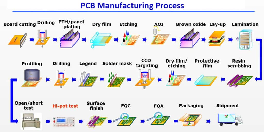
Altium is a well-known and widely used software for designing multilayer PCBs. The software provides a range of features and tools to help engineers create complex PCB designs with ease. Once the design is complete, the manufacturing process begins.
The manufacturing process for Altium multilayer PCBs typically involves the following steps:
-
Layer Stackup Design: The first step in the manufacturing process is to design the layer stackup. This involves deciding the number of layers required for the PCB and the order in which they will be stacked. Altium provides a range of layer stackup templates to choose from, which can be customized as per the project requirements.
-
Copper Cladding: Once the layer stackup is finalized, the copper cladding process begins. Copper sheets are laminated onto the substrate and then etched to create the required circuit patterns.
-
Drilling and Plating: After copper cladding, the PCB is drilled to create holes for components and vias. The holes are then plated with copper to create electrical connections between different layers.
-
Solder Mask and Silkscreen: The next step is to apply a solder mask and silkscreen to the PCB. The solder mask is applied to protect the copper traces and pads from oxidation and other environmental factors. The silkscreen is used to add text and graphics to the PCB for identification and assembly purposes.
-
Testing and Inspection: Once the PCB is complete, it undergoes rigorous testing and inspection to ensure that it meets the required specifications. This includes electrical testing, visual inspection, and automated optical inspection.
In conclusion, Altium provides a comprehensive solution for designing and manufacturing multilayer PCBs. The software’s advanced features and tools make it easy for engineers to create complex designs, and the manufacturing process ensures that the final product meets the required specifications.
Altium Multilayer PCB Design Best Practices
When designing a multilayer PCB in Altium, there are a few best practices that can help ensure success. These practices include:
1. Proper Layer Stackup
The layer stackup is crucial when designing a multilayer PCB. It is important to determine the number of layers required for the design and to properly arrange them in the stackup. This includes placing power and ground planes in the correct locations and ensuring that signal layers are properly isolated from each other.
2. Component Placement
Proper component placement is essential for signal integrity and to ensure that the board can be manufactured easily. In Altium, it is important to use the “Place Component” feature to accurately place components on the board. It is also important to follow the manufacturer’s datasheet for each component to ensure proper placement and orientation.
3. Signal Routing
Signal routing is a critical step in the design process. In Altium, it is important to use the “Interactive Routing” feature to route signals on the board. This feature allows for easy trace placement and adjustment. It is also important to use proper trace widths and spacing to ensure signal integrity.
4. Design Rule Check
Before finalizing the design, it is important to run a Design Rule Check (DRC) to ensure that the design meets all PCB manufacturing requirements. In Altium, the DRC feature can be used to check for errors such as clearance violations, trace width violations, and more.
By following these best practices, Altium users can design multilayer PCBs that are optimized for performance, manufacturability, and reliability.
