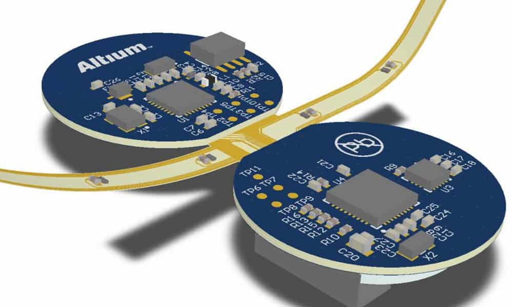
Altium PCB layout is an essential part of the printed circuit board design process. Altium is a popular software tool used by engineers and designers to create high-quality PCB layouts. The software provides a range of features that allow designers to create complex designs quickly and efficiently.
One of the key benefits of Altium PCB layout is its ease of use. The software provides a user-friendly interface that allows designers to create and edit designs quickly and easily. Additionally, Altium provides a range of templates and libraries that can be used to speed up the design process, making it an ideal tool for both experienced and novice designers.
Another advantage of Altium PCB layout is its flexibility. The software allows designers to create designs for a wide range of applications, from simple single-layer boards to complex multi-layer designs. This flexibility makes Altium an ideal tool for a wide range of industries, including aerospace, automotive, and consumer electronics. Overall, Altium PCB layout is a powerful and versatile tool that is essential for anyone involved in the design of printed circuit boards.
Overview
Altium PCB Layout is one of the most popular software tools for designing printed circuit boards (PCBs). It is a powerful and flexible tool that allows designers to create high-quality PCBs quickly and efficiently.
One of the key features of Altium PCB Layout is its user-friendly interface. The software is designed to be easy to use, even for those who are new to PCB design. It offers a wide range of tools and features that make it easy to create complex PCB designs, including schematic capture, PCB layout, and 3D visualization.
Altium PCB Layout also offers a range of advanced features that make it a powerful tool for experienced PCB designers. These features include support for high-speed design, differential pairs, and multi-board design. The software also includes a range of design rule checks (DRCs) and other tools that help ensure that the final PCB design is error-free and meets all necessary specifications.
Overall, Altium PCB Layout is a powerful and flexible tool that is ideal for both novice and experienced PCB designers. It offers a wide range of features and tools that make it easy to create high-quality PCB designs quickly and efficiently.
Designing PCB Layouts
When designing a printed circuit board (PCB), it is important to consider the various aspects of the design process to ensure a successful outcome. The PCB layout is a critical aspect of the design process that requires careful consideration and planning. In this section, we will discuss the three main stages of designing a PCB layout: schematic design, placement, and routing.
Schematic Design
The first step in designing a PCB layout is to create a schematic diagram of the circuit. The schematic diagram is a graphical representation of the circuit that shows the connections between the various components. This stage is crucial as it helps to identify any design flaws and ensures that the circuit is functioning as intended.
Placement
Once the schematic design is complete, the next step is to place the components on the PCB. The placement stage involves determining the optimal location for each component on the board. This stage is important as it can affect the overall performance of the circuit. It is important to consider factors such as signal integrity, thermal management, and accessibility when placing components.
Routing
After the components have been placed on the board, the next step is to route the traces between the components. The routing stage involves connecting the components with traces to create the desired circuit connections. This stage is important as it can affect the overall performance of the circuit. It is important to consider factors such as signal integrity, power distribution, and noise immunity when routing traces.
In conclusion, designing a PCB layout requires careful consideration and planning. The schematic design, placement, and routing stages are critical aspects of the design process that must be carefully executed to ensure a successful outcome. By following best practices and considering the various factors involved, designers can create high-quality PCB layouts that meet the needs of their projects.
Design Rule Check

Design Rule Check (DRC) is a critical process in PCB design that ensures the design meets the necessary specifications and requirements. DRC is a software tool that checks the design for errors, violations, and inconsistencies in the layout. It helps to identify and correct any design issues before the board goes into manufacturing, saving time and money.
Altium Designer provides a powerful DRC tool that helps designers to ensure the design is error-free and meets the required specifications. The tool checks the design against a set of rules defined by the designer or the manufacturer. The rules cover various aspects of the design, including trace width, clearance, spacing, drill size, and more.
The DRC tool in Altium Designer is highly customizable, allowing designers to define their own rules and constraints. The tool provides a user-friendly interface that makes it easy to set up and run the checks. The results of the DRC are displayed in a clear and concise format, making it easy for designers to identify and correct any errors.
In conclusion, the Design Rule Check is a critical process in PCB design that ensures the design meets the necessary specifications and requirements. Altium Designer provides a powerful and customizable DRC tool that helps designers to identify and correct any errors in the design before it goes into manufacturing.
Signal Integrity Analysis
Signal integrity analysis is a critical step in the PCB design process. It involves analyzing the behavior of electrical signals as they travel through a circuit, and ensuring that they maintain their integrity and quality. Poor signal integrity can lead to a range of issues, including data corruption, signal distortion, and electromagnetic interference (EMI).
To perform signal integrity analysis, designers use specialized software tools such as Altium Designer. These tools allow designers to simulate the behavior of signals in the circuit, and identify potential issues before the circuit is manufactured.
One of the key features of Altium Designer is its ability to perform pre-layout signal integrity analysis. This allows designers to identify potential issues early in the design process, and make changes before the layout is finalized. Altium Designer also includes a range of tools for post-layout signal integrity analysis, including eye diagrams, impedance analysis, and crosstalk analysis.
Another important aspect of signal integrity analysis is the use of controlled impedance routing. This involves ensuring that the impedance of the transmission lines in the circuit is consistent, which helps to maintain signal integrity. Altium Designer includes a range of tools for controlled impedance routing, including an impedance calculator and an impedance profile editor.
In conclusion, signal integrity analysis is a critical step in the PCB design process, and can help to ensure that circuits function correctly and reliably. Altium Designer provides a range of tools for signal integrity analysis, including pre-layout and post-layout analysis, as well as tools for controlled impedance routing. By using these tools, designers can identify and address potential signal integrity issues, and create high-quality, reliable PCB layouts.
3D Visualization
Altium PCB Layout offers a 3D visualization tool that allows you to view your design in a three-dimensional space. This feature is useful for checking the placement of components, identifying potential interference issues, and ensuring that everything fits together properly.
The 3D visualization tool is easy to use and provides a realistic representation of your design. You can rotate the view, zoom in and out, and even perform virtual walkthroughs of your design. This makes it easy to spot any potential issues and make adjustments before sending your design to production.
One of the benefits of the 3D visualization tool is that it allows you to view your design from any angle. This is particularly useful when working with complex designs that have multiple layers. You can easily switch between different layers to see how they fit together and identify any potential issues.
Another benefit of the 3D visualization tool is that it allows you to check the placement of components. You can easily see if components are too close together or if there are any potential interference issues. This can save you time and money by identifying issues before production.
In conclusion, the 3D visualization tool in Altium PCB Layout is a powerful feature that can help you identify potential issues and ensure that your design is ready for production. By using this tool, you can save time and money by catching issues before they become a problem.
Manufacturing Outputs
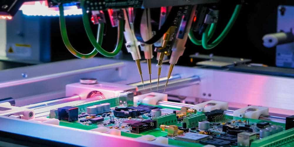
Once the PCB design is complete, the next step is to generate the manufacturing outputs. These outputs are the files that provide the necessary information for the PCB manufacturer to fabricate and assemble the board. Altium Designer offers a variety of manufacturing outputs to ensure that your design is accurately translated into a physical product.
The manufacturing outputs in Altium Designer include:
-
Gerber files: These files contain the information necessary for the PCB manufacturer to create the copper traces, pads, and vias on the board.
-
NC Drill files: These files provide the drill locations and sizes for the holes on the board.
-
Bill of Materials (BOM): This file lists all the components used in the design, along with their part numbers, quantities, and reference designators.
-
Assembly drawings: These drawings provide a visual representation of the assembled board, including the location of each component.
-
Pick and Place files: These files provide the location and orientation information for each component on the board.
Altium Designer also offers the ability to customize the manufacturing outputs to meet the specific requirements of your PCB manufacturer. This can include adding custom notes or instructions, modifying the layer stack-up, or adjusting the board dimensions.
In conclusion, Altium Designer provides a comprehensive set of manufacturing outputs to ensure that your design is accurately translated into a physical product. With the ability to customize these outputs, you can ensure that your PCB manufacturer has all the information necessary to fabricate and assemble your board with precision and accuracy.
