Amplifier printed circuit boards play a vital role in the design process of certain electronic devices. The amplifier circuit board is often referred to as the heart of the amplifier, containing components that accept a signal.
The amplifier increases its strength by passing the signal through an integrated circuit, transistor, or tube with additional current from a power supply. Amplifiers are useful in a wide range of things, including sound production; that’s why they are present in sound-making devices.
PCBs or circuit boards come in different sizes and capabilities, but they all typically contain components soldered to a substrate. More often than not, engineers often ignore the layout of a PCB in the circuit design problem.
Different problems can arise from this, like the circuit’s schematic being correct but not working or running at low performance. In this article, we will discuss what an amplifier Printed Circuit Board is, its functions and characteristics, and how to wire the layout.
What Is an Amplifier Printed Circuit Board?
An amplifier printed circuit board (or amplifier PCB) is a circuit board that produces an enhanced signal fed into input terminals. Naturally, an amplifier Printed Circuit Board features electronic components that can accept a signal and are able to enhance the amplifier’s strength.
They are able to do this by passing the signal fed into terminals through a tube or transistor. Amplifier PCBs, like those used in professional audio devices or for home audio systems, tend to be very large, measuring up to 100 square inches. However, the ultra compact design is what differentiates it from a guitar amplifier or audio amplifiers used in making home theater systems.
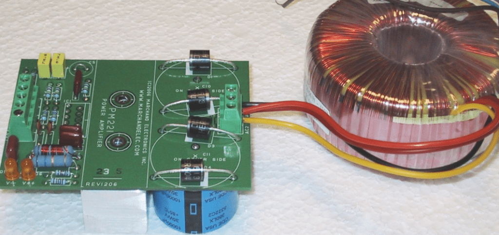
More often than not, PCBs lack a very essential component: power supply; in battery-powered amplifiers, the battery supplies the power. However, the majority of small amplifiers utilizes or integrates an external power supply. Amplifier printed circuit boards are of two major types: audio amplifiers and power amplifier boards.
How Important is an Audio Amplifier PCB?
An audio amplifier is that simple circuit design needed to amplify an audio signal received from devices like microphones or speakers. The amplifier is very crucial in the design of an audio amplifier or Wi-Fi amplifier; the circuit layout must generate and enhance the signal. If there is a bad configuration, it can mean scattered capacitors, leak resistances, uneven diodes, or voltage slips during the amplifier Printed Circuit Board phase.
The amplifier circuit board generates a boosted variation of an input signal that has been loaded into its input port. It is essential that one gets the configuration of an audio or Wi-Fi amplifier right to avoid ruining the entire project.
What is an Amplifier PCB Layout?
The layout of an amplifier printed circuit board refers to a graphic drawing of copper wire designs performed on a board layout. In other words, the amplifier PCB design layout is a schematic drawing of copper wiring patterns found on circuit boards. The design layout is created using a PCB builder. This is a mechanism that enables the amplifier Printed Circuit Board to boost whatever the quantity of input signals loaded into it.
In many situations, amplifier Printed Circuit Board serves as the primary action point for turning analog signals into digital signals. First, they amplify the signals; then, they analyze them using a microprocessor to generate an output. Amplifier PCB layouts serve as a bridge between the receiver and the circuitry, aiding in the prevention of unintended signals.
What Are the Benefits of PCB Layout of Amplifiers?
An amplifier PCB layout is considered to have an improved power quality and feedback loop. Also, they are quite easy and simple to put together, with only a small number of parts and a single unit. Furthermore, amplifier PCB layout devices relay half of a half-wave; thus, they result in a complete current needed to drive the load. This makes the configuration of the amplifier PCB much more effective.
Also, the PCB layout of the amplifier is referred to as an alternative solution as the amplifier is capable of removing cross-over distortion. Plus, the amplifier PCB layout has a greater frequency than others; to get 80% reliability, you have to rely on radio frequency adjust activities.
What Are the Downsides of Amplifier PCB Layouts?
In some situations, PCB traces are incorrectly installed, which means you have to regularly solder during the removal and replacement of output components. As a result, there is a great chance of causing damage to parts of the PCB or even outright wreckage of the PCB structure. Another downside is that the output devices tend to get very hot, particularly if overheating is not managed by heat sinks.
Meanwhile, the heat sinks will only work if they are correctly fitted. Overheating is very likely even if the PCB has a decent run in its scores. Moreover, since the printed circuit board will potentially produce a greater current, overheating is inevitable in amplifiers
.
Layout Conventions for Laying Out Amplifier Printed Circuit Boards
After carefully selecting the appropriate collection of parts for the amplifier PCB, the next crucial step is the layout. The PCB layout is essential as it enables the computer to provide the optimal output that is required for the specific system.
For instance, if you want to have an optimized home theater system structure, you need about 6 epoxy-filled layers. If you are laying out a PCB, you should first ensure you minimize the connection of the inverting pins.
Also, ensure you place the decoupling capacitor as close to the power supply pin as possible. If you are using multiple decoupling capacitors, ensure the smallest decoupling capacitor is placed closest to the power supply pin.
Additionally, be careful not to place the vials between the power supply pins and the decoupling capacitor. Last but not least, keep the routing path as wide as possible; expand it as much as you can.
How Should You Install the Power of a Plane?
Install the power planes thick enough to bring the needs of the existing supply pin up to the limit. The best way to do this is to trace the planes to various ICs in the star-connectedly, starting from the power control IC. Designing the layout this way mitigates the negative impact on other ICs which is created by the high switching ICs same-line exchange.
Using bypass transistors is recommended because it aligns with the instant switching current needs of the particular design. Also, bypass transistors help to detach voltage noise disturbances on control pins, ensuring a stable and steady power supply and enhanced efficiency.
Placing the capacitors close to the appropriate pin on the top layer helps to minimize redundant inductors and routing resistance. Consider routing the internal pins from the immediate layer to the top layer to minimize parasitic effects where the decoupling capacitor is inaccessible.
The Best Position for the Capacitor
The way the capacitor is positioned matters to prevent spurious inductors. The capacitor should be placed as close to a certain pin on the top layer as possible. Resistors and inductors will likely cause voltage spike undershoot or overshoot due to switching current needs. The voltage surge is as a result of the swapping of the current needs of the power supplies.
Voltage ripple and system activity impediment can be caused by even inductors because of the sudden number needed. Also, another way to minimize parasitic inductance and resistance is having the shortest resistance diverging route.
You are expected to place the smallest decoupling cap close to the unit pin and that distance should not exceed 1 mm. If there are additional caps, they are to be placed as close to the unit pin as possible.
Signal Switch and Charge Pump Capacitor
There should be a redirection of the constant switch signals from SW node, class-D output, and signals using the board power supply rectifier. This is to enable them to interfere with each other or another signal on the PC and also to prevent coupling or other interferences with the power supplies. However, they should not be routed in the same layer as other signals, especially if there is no ground protection between the layers.
For the charge pump capacitor, there should be very low parasitic inductance and resistance between the PVDD pin and the GREG/VREG pin. Also, there should be a start connection of the charge pump capacitor as close to the PVDD pin (not plane) as possible. Use thick routing and immediate for signal routing to minimize parasitic on the pin.
Transmitting Class-D Output Signals and Routing Digital Signals
Class-D output signals have to be transmitted in two layers within at least thirty miles. As far as EM specifications go, every output is directed sixty miles wide to the speaker. If you are using an EMI filter, position it as near to the unit pins as possible. Also, ensure the output signals are length-matched to each other to prevent discrepancy damage from routing resistance differences.
Meanwhile, there is a specific way signals in digital format must be routed to protect their dignity and avoid conflict with other signals. Essentially, you want to ensure the signals are not connected to any swapping nets. If this happens, the digital signals will pair up and start injecting noise.
What Is the Difference between Normal PCBs and Amplifier PCBs?
Normal PCBs and amplifier PCBs are different in many ways, including their manufacturing. In a normal PCB, through-hole or surface mount technology is used to mount PCB components and drill holes onto the circuit board.
In amplifier PCBs, however, manufacturing is done through a schematic capture, where EasyEDA is used to place components. Furthermore, the physical aspects of the board are determined by the complexity of the circuit. The amplifier PCBs also come with speaker protection boards, a heavy duty rectifier, a power amplifier board, and an output short circuit protection.
Placing components in an amplifier Printed Circuit Board requires paying attention to some very crucial factors, including thermal and geometry factors. Also, the power input and output in amplifier PCBs function in response with the transistors’ response.
Overall, the dielectric constant in an amplifier Printed Circuit Board is better than the one in a normal PCB. Nevertheless, both PCBs utilize schematic diagrams in their design, although a normal PCB can be designed manually with a Photomask.
What Are the Characteristics of Amplifier PCBs?
Amplifier PCBs have high input impedance, limited bandwidth, high open-loop gain, and low output impedance. The high-input impedance, for instance, helps the voltage to drop entirely on the amplifier and helps avoid loading. Also, in amplifier PCBs, the signal amplifies when the voltage drops, which can lead to signal loss across the fed device.
Amplifier PCBs can enhance the power of a signal, which can be measured between the output and input ports. Furthermore, the high open-loop gain in amplifier PCBs ensures many feedback levels. The most important thing is knowing how to assemble the features of these circuits to achieve the desired support at a low cost.
So whether you are working on hobby projects, led indicators, studio amplifiers, mosfet amplifiers, graphic equalizers, subwoofer amps, home theater systems, audio amplifiers, or other standard components, amplifier PCBs are a great choice. The working voltage, high current, compact size of box, price, and other features makes it a suitable choice.
Conclusion
Amplifier Printed Circuit Boards are used and beneficial in many applications; they serve a wide range of purposes. To start with, they are the major points of operation when changing analog signals to digital signals.
Amplifier PCBs help enhance the amplitude of signals while maintaining other aspects such as the frequency. Additionally, amplifier PCBs can transform analog signals not only to digital signals but also to square waves, thanks to the transformers they possess that allows for a seamless signal conversion on the channel.
With its high voltage and high output resistance, an amplifier circuit board offers adequate output to drive loudspeakers while providing the necessary filters needed by the car, transformer, or other electronics that work with it. Furthermore, amplifier PCBs are essential in identifying metal fatigue; they also help in ultrasonic cleaning and ultrasound scanning. Amplifier printed circuit boards, particularly those with a constant gain control between DC and AC, are very useful in oscilloscopes.
