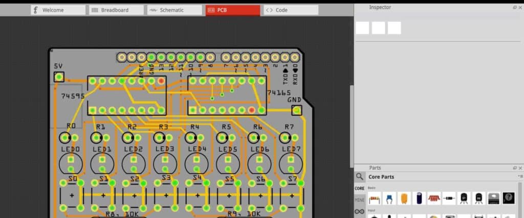
Automatic PCB design is a process that involves using software to create printed circuit board layouts without the need for manual intervention. This process can save time and reduce errors as it eliminates the need for human input in the design process. The use of automatic PCB design software has become increasingly popular in recent years due to its ability to streamline the design process and produce high-quality PCB layouts.
One of the key benefits of automatic PCB design is its ability to reduce design time. With traditional PCB design methods, designers would need to manually place components and route traces, which could take a significant amount of time. However, with automatic PCB design software, the process is much faster and more efficient. This allows designers to focus on other important aspects of the design, such as optimizing the circuit layout or ensuring that the board meets specific requirements.
Overall, automatic PCB design has become an essential tool for PCB designers looking to streamline the design process and produce high-quality PCB layouts. With its ability to reduce design time, eliminate errors, and improve overall design quality, automatic PCB design software is a valuable asset for any designer looking to create complex PCB layouts quickly and efficiently.
What is Automatic PCB Design?
Automatic PCB design is a process of designing printed circuit boards (PCBs) using software tools that automate the majority of the design process. These software tools are capable of generating schematics, laying out components, routing traces, and generating manufacturing files automatically.
Automatic PCB design software can be used to design simple to complex PCBs, including multi-layer boards, with minimal human intervention. The software can also perform design rule checks (DRCs) to ensure that the design meets industry standards and is manufacturable.
The use of automatic PCB design software can significantly reduce the time and effort required to design a PCB, as well as reduce the likelihood of errors and inconsistencies in the design. This can lead to faster product development and a more efficient design process.
Some benefits of automatic PCB design include:
- Faster design process: Automatic PCB design software can quickly generate a design based on a set of requirements, reducing the time required for manual design.
- Improved accuracy: The software can ensure that the design meets industry standards and is manufacturable, reducing the likelihood of errors and inconsistencies.
- Increased productivity: Automatic PCB design can free up engineers’ time to focus on other aspects of the product development process.
Overall, automatic PCB design is a valuable tool for designers looking to streamline the PCB design process and improve productivity.
Advantages of Automatic PCB Design

Automatic PCB design is becoming increasingly popular in the electronics industry due to its numerous advantages over manual design. Here are some of the key benefits of using automatic PCB design software:
-
Faster Design Process: Automatic PCB design software can significantly reduce the time needed to design a PCB. With automated tools for routing, placement, and optimization, designers can complete their work much more quickly than if they were doing everything manually.
-
Improved Accuracy: Automatic PCB design software is highly accurate, which helps to reduce errors and improve the quality of the final product. This is especially important in complex designs where even small mistakes can have a significant impact on performance.
-
Cost Savings: By reducing the time and effort required to design a PCB, automatic design software can help to lower costs. Additionally, the improved accuracy of the software can reduce the need for costly rework and redesigns.
-
Ease of Use: Many automatic PCB design tools are designed to be easy to use, even for those with limited experience in PCB design. This makes it possible for more people to create high-quality PCBs without having to spend years learning the ins and outs of manual design.
-
Flexibility: Automatic PCB design software is highly flexible, allowing designers to quickly make changes and adjustments to their designs as needed. This can be especially useful in situations where a design needs to be modified quickly in response to changing requirements.
Overall, automatic PCB design offers a number of advantages over manual design, including faster design times, improved accuracy, cost savings, ease of use, and flexibility. As a result, it is becoming an increasingly popular choice for electronics designers looking to create high-quality PCBs quickly and efficiently.
Challenges in Automatic PCB Design
Automatic PCB design is a complex process that involves many challenges. Here are some of the most common challenges that designers face:
Component Placement
One of the biggest challenges in automatic PCB design is component placement. This is particularly true for designs that have a large number of components. The placement of components on the board can have a significant impact on the performance of the circuit, and it can be difficult to optimize the placement of components manually.
Routing
Routing is another major challenge in automatic PCB design. The routing of traces on the board can have a significant impact on the performance of the circuit. However, routing can be a time-consuming and complex process, particularly for designs that have a large number of components.
Design Rules
Design rules are another challenge in automatic PCB design. Design rules are used to ensure that the design meets specific requirements, such as minimum trace width, minimum clearance, and maximum current density. However, it can be difficult to define design rules that are appropriate for a specific design.
Design for Manufacturability
Design for manufacturability is an important consideration in automatic PCB design. The design must be optimized for the manufacturing process, which can include considerations such as panelization, solder mask, and copper plating.
Design Validation
Design validation is another challenge in automatic PCB design. The design must be validated to ensure that it meets specific requirements, such as electrical performance and reliability. However, it can be difficult to validate the design, particularly for complex designs.
In conclusion, automatic PCB design is a complex process that involves many challenges. Component placement, routing, design rules, design for manufacturability, and design validation are just a few of the challenges that designers face. However, with the right tools and techniques, these challenges can be overcome, and high-quality PCB designs can be produced.
Tools for Automatic PCB Design
When it comes to designing printed circuit boards (PCBs), modern software tools have made the process much easier and faster. Automatic PCB design tools are becoming increasingly popular as they allow designers to create high-quality PCBs quickly and efficiently. Here are some of the most popular tools for automatic PCB design:
1. Altium Designer
Altium Designer is a popular PCB design tool that offers a range of features for both beginners and experienced designers. It includes a schematic editor, PCB editor, and a library of over 350,000 components. Altium Designer also offers advanced features such as 3D visualization and simulation tools.
2. Eagle PCB Design
Eagle PCB Design is another popular tool for automatic PCB design. It has a user-friendly interface and allows designers to create schematics, layout PCBs, and generate Gerber files. Eagle PCB Design also offers a large library of components, making it easy for designers to find the parts they need.
3. KiCAD
KiCAD is a free and open-source PCB design tool that has gained popularity in recent years. It includes a schematic editor, PCB layout editor, and a 3D viewer. KiCAD also offers a large library of components and supports a range of file formats.
4. CircuitMaker
CircuitMaker is a free PCB design tool that offers a range of features for both beginners and experienced designers. It includes a schematic editor, PCB layout editor, and a library of over 350,000 components. CircuitMaker also offers advanced features such as 3D visualization and simulation tools.
5. EasyEDA
EasyEDA is a cloud-based PCB design tool that allows designers to create schematics, layout PCBs, and generate Gerber files. It also offers a large library of components and supports a range of file formats. EasyEDA is free to use, but it also offers a paid version with additional features.
In conclusion, these are some of the most popular tools for automatic PCB design. Each tool has its own unique features and benefits, so designers should choose the tool that best suits their needs. With the help of these tools, designers can create high-quality PCBs quickly and efficiently.
How to Choose the Right Automatic PCB Design Tool
Choosing the right automatic PCB design tool is crucial for creating high-quality printed circuit boards. Here are some factors to consider when selecting a tool:
1. Features
The first thing to consider is the features offered by the tool. Different tools have different capabilities, so it’s essential to choose one that meets your specific needs. Some essential features to look for include:
- Design rule checks
- Auto-routing
- 3D visualization
- Gerber file generation
- Schematic capture
2. Ease of Use
Another important factor to consider is the ease of use of the tool. A tool that is difficult to navigate and use can lead to errors and frustration. Look for a tool that has an intuitive interface and provides clear instructions.
3. Compatibility
Make sure the tool you choose is compatible with the operating system you are using. Some tools are only available for Windows, while others are only available for Mac or Linux. Also, check the compatibility of the tool with the file formats you will be using.
4. Price
Finally, consider the price of the tool. Automatic PCB design tools can range from free to several thousand dollars. Determine your budget and choose a tool that fits within it. Keep in mind that some tools may require additional add-ons or modules, which can add to the overall cost.
By considering these factors, you can choose the right automatic PCB design tool that meets your needs and helps you create high-quality printed circuit boards.
Designing PCBs with Automatic PCB Design Tools

Designing printed circuit boards (PCBs) is a critical step in the electronics design process. Traditionally, PCB design has been a time-consuming and error-prone process that requires specialized knowledge and expertise. However, with the advent of automatic PCB design tools, designing PCBs has become faster and easier than ever before.
Automatic PCB design tools use algorithms and rules-based systems to generate PCB layouts automatically. These tools can significantly reduce the time and effort required to design a PCB, while also improving the accuracy and quality of the final design. Some of the benefits of using automatic PCB design tools include:
- Faster design times: Automatic PCB design tools can generate PCB layouts in a fraction of the time it would take a human designer to do the same job.
- Improved accuracy: Automatic PCB design tools can ensure that the PCB layout meets all design specifications and requirements, reducing the risk of errors and mistakes.
- Increased productivity: By automating the PCB design process, designers can focus on other aspects of the design process, such as circuit design and testing.
- Cost savings: By reducing the time and effort required to design a PCB, automatic PCB design tools can help to lower overall design costs.
When using automatic PCB design tools, designers typically start by specifying the design parameters and constraints, such as the size and shape of the PCB, the number and type of components, and the desired signal routing. The software then generates a PCB layout that meets these requirements, using algorithms and rules-based systems to optimize the layout for performance, manufacturability, and cost.
Overall, automatic PCB design tools are a valuable asset for electronics designers, enabling them to create high-quality PCB layouts quickly and efficiently. By reducing the time and effort required to design a PCB, these tools can help designers to focus on other aspects of the design process, such as circuit design and testing, ultimately leading to faster time-to-market and improved product quality.
Conclusion
In conclusion, automatic PCB design software has revolutionized the way electronic engineers design and manufacture printed circuit boards. With the use of these tools, engineers are able to quickly create complex designs, reduce errors and costs, and improve the overall quality of their products.
One of the key benefits of automatic PCB design software is the ability to reduce the time it takes to design a board. These tools provide a comprehensive set of features that allow designers to easily create and modify their designs, eliminating the need for manual calculations and repetitive tasks.
Another advantage of automatic PCB design software is the reduction in errors. These tools have built-in checks and balances that help to catch mistakes before they become costly problems. This not only saves time and money but also improves the reliability of the final product.
Finally, automatic PCB design software has improved the overall quality of electronic products. With the ability to create more complex designs, engineers are able to create products that are more efficient, reliable, and cost-effective. This has led to increased customer satisfaction and improved brand reputation.
Overall, automatic PCB design software is an essential tool for electronic engineers looking to design and manufacture high-quality products. With its ability to reduce design time, eliminate errors, and improve product quality, it is no wonder that these tools have become an industry standard.
