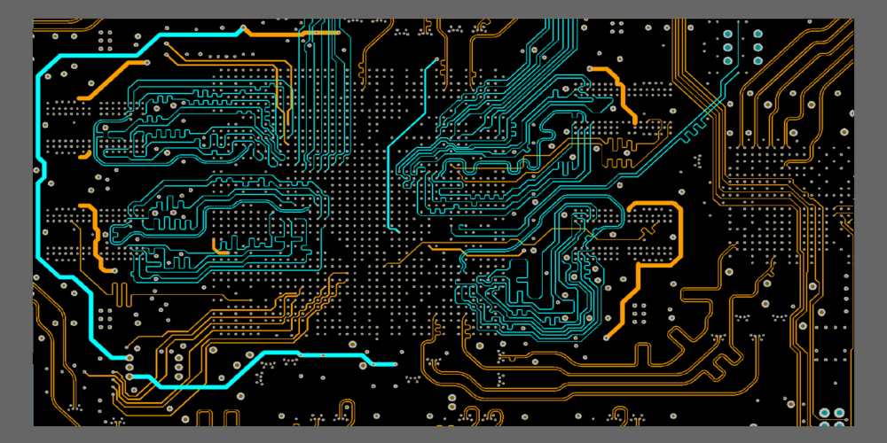
Board design layout is an essential aspect of creating electronic devices. The layout of the board determines how the various components and circuits are arranged to ensure optimal functionality. A poorly designed board can lead to a range of issues, including reduced performance, increased power consumption, and even complete failure.
When designing a board layout, it is essential to consider factors such as signal integrity, power distribution, and thermal management. Each component must be placed in the optimal location to ensure the smooth flow of signals and power. The layout must also be optimized to minimize thermal hotspots and ensure that components do not overheat.
Overall, board design layout is a critical aspect of creating electronic devices. A well-designed board layout can ensure optimal performance and reliability, while a poorly designed one can lead to a range of issues. By considering factors such as signal integrity, power distribution, and thermal management, designers can create boards that meet the needs of their specific applications.
Basics of Board Design Layout
Board design layout is the process of arranging electronic components and their interconnections on a printed circuit board (PCB). A well-designed layout is crucial for the proper functioning of electronic circuits and can significantly affect their performance.
The following are some basic guidelines to keep in mind when designing a board layout:
-
Component Placement: Components should be placed in a logical and organized manner to minimize the length of the interconnects and reduce the overall board size. Grouping similar components together can also help in reducing noise and interference.
-
Signal Traces: Signal traces should be kept as short as possible to minimize signal degradation and interference. Traces carrying high-speed signals should be routed as differential pairs to reduce crosstalk.
-
Power and Ground: Proper grounding and power distribution are critical for the proper functioning of electronic circuits. Ground and power planes should be used to provide a low-impedance path for current flow.
-
Thermal Management: Electronic components generate heat, and proper thermal management is essential to prevent overheating and component failure. Heatsinks, thermal vias, and thermal pads can be used to dissipate heat.
-
Design for Manufacturability: The board layout should be designed keeping in mind the manufacturing process. Components should be placed in a way that makes them easy to assemble, and the board should be designed to minimize the number of manufacturing steps.
In conclusion, the board design layout is a critical aspect of electronic circuit design that should not be overlooked. By following some basic guidelines, designers can create a well-organized and optimized layout that ensures proper functioning of electronic circuits.
Factors to Consider in Board Design Layout

When designing a printed circuit board (PCB), there are several factors to consider to ensure that the final product meets the required specifications. Here are some of the most important factors to keep in mind:
Component Placement
The placement of components on a PCB is critical to its overall performance. Components should be placed in a way that minimizes noise and signal interference. High-speed digital components should be placed as close to the power source as possible, while analog components should be placed away from digital components to minimize noise.
Power and Ground Planes
Power and ground planes are essential for providing stable power and minimizing noise. The power plane should be placed adjacent to the ground plane to minimize the inductance of the power supply. The power and ground planes should be connected with multiple vias to ensure a low impedance connection.
Trace Routing
Trace routing is the process of laying out the interconnections between components on a PCB. The routing should be done in a way that minimizes the length of the traces and the number of vias. High-speed signals should be routed as short and direct as possible to minimize signal reflection and crosstalk.
Thermal Management
Thermal management is essential for ensuring the reliability of a PCB. Heat-generating components should be placed in areas with good airflow, and thermal vias should be used to dissipate heat away from critical components. Thermal relief pads should be used for components that require heat dissipation.
Design for Manufacturability
Design for manufacturability (DFM) is the process of designing a PCB with the manufacturing process in mind. The design should be optimized for the manufacturing process to minimize the cost and time required to produce the PCB. DFM guidelines should be followed to ensure that the PCB can be manufactured reliably and efficiently.
In summary, when designing a PCB, it is essential to consider component placement, power and ground planes, trace routing, thermal management, and design for manufacturability. By keeping these factors in mind, designers can create a PCB that meets the required specifications and is reliable and efficient to manufacture.
Tools and Techniques for Board Design Layout
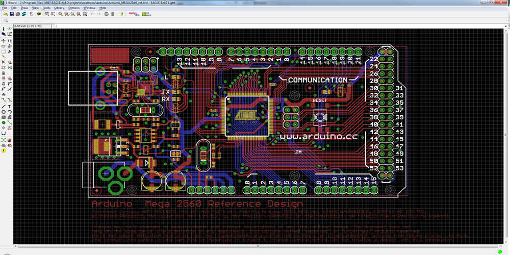
When it comes to designing a printed circuit board (PCB), there are a variety of tools and techniques available to help you create a successful layout. Here are a few key tools and techniques to keep in mind:
Tools
-
Schematic capture software: This software allows you to create a schematic of your circuit design, which can then be used to create a layout in a PCB design tool.
-
PCB design software: There are many PCB design tools available, from free open-source options to professional-grade software. Some popular options include Eagle PCB, Altium Designer, and KiCad.
-
Simulation software: Simulation software can be used to test your circuit design before creating a physical prototype. This can help you catch errors and optimize your design before moving forward.
Techniques
-
Component placement: Careful placement of components on your PCB can help minimize noise and interference, as well as optimize signal flow.
-
Routing: Routing refers to the process of connecting the components on your PCB with traces. It’s important to pay attention to trace width, spacing, and placement to ensure proper signal flow.
-
Ground planes: Ground planes are large areas of copper on your PCB that are connected to ground. These can help reduce noise and interference in your circuit.
-
Signal integrity analysis: Signal integrity analysis can help you identify issues with signal quality and optimize your design for better performance.
By utilizing these tools and techniques, you can create a successful PCB layout that meets your specific design requirements.
Designing for Manufacturing and Assembly
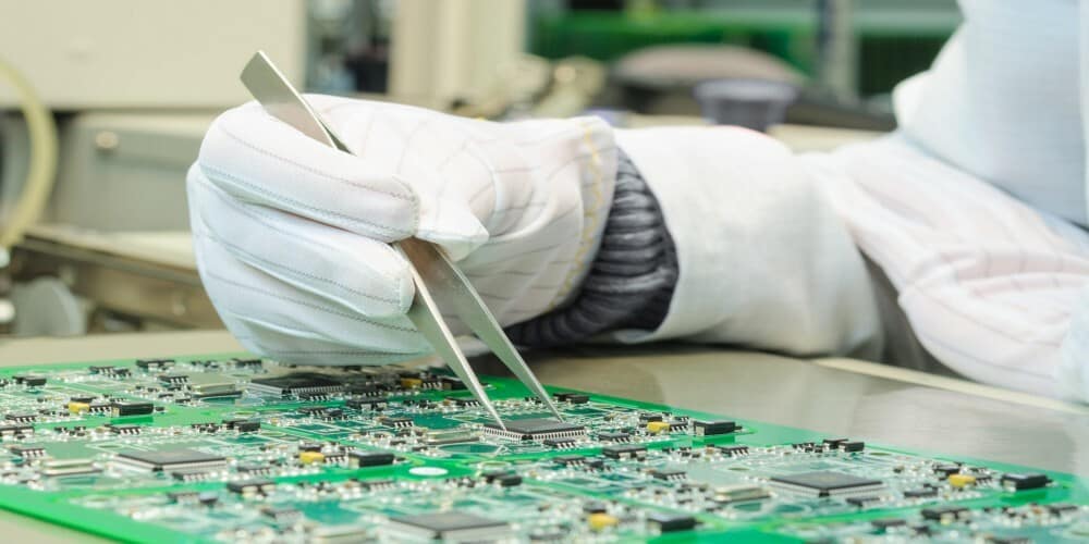
When designing a board layout, it’s essential to consider the manufacturing and assembly process. By designing with these factors in mind, you can reduce the risk of errors and improve the efficiency of the production process.
Here are some key considerations when designing for manufacturing and assembly:
-
Component Placement: Placing components in a logical and organized manner can help reduce the assembly time and minimize the risk of errors. Grouping similar components together and placing them in a way that allows for easy access during assembly can help streamline the process.
-
Clear Labeling: Clear, concise labeling of components and their placement on the board can help eliminate confusion during assembly. Using unique identifiers for each component and labeling them in a consistent manner can help ensure that the correct components are used in the right places.
-
Standard Components: Using standard components can help simplify the manufacturing process. Standard components are readily available, which can help reduce lead times and lower costs. They are also easier to assemble, reducing the risk of errors.
-
Design for Testability: Designing for testability can help reduce the time and cost of testing. By including test points and access to critical signals, you can simplify the testing process and reduce the risk of errors.
-
Design for Manufacturability: Designing for manufacturability involves considering the manufacturing process when designing the board. By designing with the manufacturing process in mind, you can reduce the risk of errors, improve the efficiency of the production process, and lower costs.
By considering these factors when designing a board layout, you can help ensure that the manufacturing and assembly process is efficient and error-free.
Testing and Verification of Board Design Layout
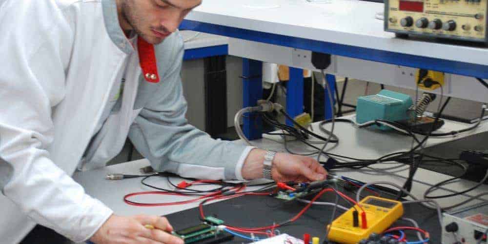
After the board design layout has been completed, it is essential to conduct rigorous testing and verification to ensure that the board functions as intended. Testing and verification help to identify and correct any design flaws, errors, or omissions before the board is manufactured.
One of the most critical aspects of testing and verification is the use of simulation tools. These tools allow designers to simulate the behavior of the board in different operating conditions and identify any potential issues. Simulation tools also help to optimize the design for performance, power consumption, and cost.
Another crucial aspect of testing and verification is the use of physical prototypes. Physical prototypes allow designers to test the board’s functionality in real-world conditions and identify any issues that may not have been detected during simulation. Physical prototypes also help to validate the design and ensure that it meets the required specifications.
In addition to simulation and physical prototyping, designers must also conduct a series of tests to verify the board’s functionality. These tests may include power-on self-test (POST), boundary scan testing, functional testing, and environmental testing. The results of these tests help to identify any design flaws or errors that need to be corrected.
Overall, testing and verification are critical components of the board design process. By using simulation tools, physical prototypes, and a series of tests, designers can ensure that the board functions as intended and meets the required specifications.
