KiCad PCB from schematic is a popular open-source software suite that allows users to design printed circuit boards (PCBs) from schematics. It is a powerful tool that provides an extensive set of features, including a schematic editor, a PCB layout editor, and a 3D viewer. With KiCad, users can create professional-grade PCB designs for various applications.
One of the most significant advantages of using KiCad PCB from schematic is its open-source nature. This means that the software is entirely free to use and can be modified to suit individual needs. Additionally, KiCad is available for all major operating systems, including Windows, macOS, and Linux, making it an accessible option for a wide range of users. Whether you are a hobbyist or a professional, KiCad provides a flexible and customizable platform for designing PCBs.
Overall, KiCad PCB from schematic is an excellent tool for designing PCBs. With its open-source nature, extensive feature set, and cross-platform compatibility, it is a versatile option for anyone looking to create high-quality PCB designs. Whether you are just starting or have years of experience, KiCad is a reliable and efficient choice that can help you bring your ideas to life.
Creating a Schematic in KiCad
Adding Components to the Schematic
To create a schematic in KiCad, the first step is to add components to the schematic sheet. In the schematic editor, click on the “Place Symbol” button to open the component library. Browse the library to find the desired component and click on it to select it. Then, place the component on the schematic sheet by clicking on the desired location.
After placing the component, you can adjust its properties by double-clicking on it. This will open the component properties dialog box, where you can modify the component’s values, footprint, and other parameters.
Connecting Components with Nets
Once the components are placed on the schematic sheet, the next step is to connect them with nets. Nets represent the electrical connections between components. To create a net, click on the “Place Net” button and draw a line between the pins of the components that need to be connected.
To rename a net, double-click on it and enter a new name in the “Net Name” field. You can also add labels to the net by clicking on the “Place Label” button and typing in the desired text.
It is important to ensure that all the components are correctly connected with nets, as any missing connections can result in errors during the PCB layout process.
Overall, creating a schematic in KiCad is a straightforward process that involves adding components to the schematic sheet and connecting them with nets. By following these simple steps, you can create a clear and accurate schematic that will serve as the foundation for your PCB design.
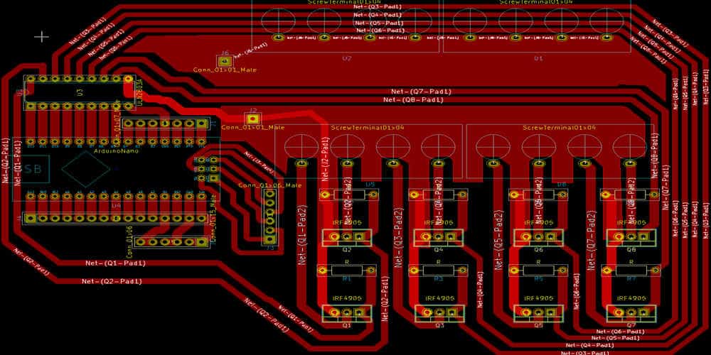
Creating a PCB Layout from a Schematic

Generating Netlist
Before creating a PCB layout from a schematic, the first step is to generate a netlist. A netlist is a list of all the connections between the components in the schematic that need to be routed on the PCB. To generate a netlist, open the schematic in KiCad and go to the “Tools” menu. From there, select “Generate Netlist” and choose the appropriate options for your PCB design.
Importing Netlist into PCB Layout Editor
Once the netlist is generated, the next step is to import it into the PCB layout editor. To do this, open the PCB layout editor in KiCad and go to the “File” menu. From there, select “Import Netlist” and choose the netlist file that was generated from the schematic.
After importing the netlist, the components will appear on the PCB layout editor canvas. The next step is to arrange the components and route the connections between them. KiCad provides a variety of tools to help with this process, including automatic routing and design rule checking.
It is important to note that the PCB layout should be designed with the physical constraints of the PCB in mind, such as the size and shape of the board, the placement of the components, and the routing of the traces. It is also important to follow best practices for PCB layout design, such as minimizing the length of traces and avoiding crossing traces.
Overall, creating a PCB layout from a schematic in KiCad is a straightforward process that can be accomplished with a few simple steps. By following best practices and utilizing the tools provided by KiCad, it is possible to create a high-quality PCB layout that meets the requirements of your design.
Placing Components on the PCB

Manually Placing Components
Manually placing components on a PCB can be a time-consuming process, but it allows for greater control over the placement of components. When placing components manually, it is important to keep in mind the spacing between components, the orientation of polarized components, and the overall layout of the PCB.
To manually place components on a PCB in KiCad, follow these steps:
- Open the PCB layout editor by clicking on the “Pcbnew” button in the KiCad main menu.
- Click on the “Place Footprint” button in the toolbar to open the component placement dialog box.
- Select the component you want to place from the list of available footprints.
- Click on the location on the PCB where you want to place the component.
- Repeat steps 3 and 4 for each component you want to place.
Using Automated Placement Tools
Automated placement tools in KiCad can speed up the process of placing components on a PCB by automatically placing components based on a set of predefined rules. These tools can be useful for quickly laying out a PCB, but may not always result in the most optimal placement of components.
To use the automated placement tools in KiCad, follow these steps:
- Open the PCB layout editor by clicking on the “Pcbnew” button in the KiCad main menu.
- Click on the “Tools” menu and select “Update PCB from Schematic” to update the PCB layout based on the schematic.
- Click on the “Tools” menu and select “Run PCBNew Auto-Placer” to open the automated placement tool.
- Set the placement options, such as the number of iterations and the placement strategy.
- Click on the “Run” button to start the automated placement process.
In conclusion, both manual and automated placement methods have their advantages and disadvantages. It is up to the designer to decide which method to use based on the specific requirements of the PCB design.
Routing the PCB
Once you have completed the schematic design, the next step is to route the PCB. Routing is the process of creating physical connections between the components on the PCB. In this section, we will discuss two methods of routing the PCB: manual routing and using automated routing tools.
Manual Routing
Manual routing involves physically drawing the traces on the PCB layout. This process can be time-consuming, but it allows for greater control over the routing process. When manually routing the PCB, it is important to keep in mind the following:
- Keep traces as short as possible to reduce noise and interference
- Avoid crossing traces to prevent signal crosstalk
- Use wider traces for power and ground connections to reduce resistance
- Place components as close together as possible to reduce trace length
Using Automated Routing Tools
Automated routing tools can help speed up the routing process by automatically generating the traces for you. These tools use algorithms to determine the best routing path based on the design rules and constraints you set. When using automated routing tools, it is important to keep in mind the following:
- Set design rules and constraints to ensure the tool generates a layout that meets your requirements
- Check the generated layout to ensure it meets your design specifications
- Use the tool to generate a preliminary layout, then manually adjust the traces as needed
In summary, both manual routing and automated routing tools have their advantages and disadvantages. Manual routing provides greater control but can be time-consuming, while automated routing tools can speed up the process but may require manual adjustments. Ultimately, the choice of routing method will depend on your design requirements and personal preference.
Design Rule Check (DRC)

Running DRC Checks
Before sending your KiCad PCB design to the manufacturer, it’s essential to run a Design Rule Check (DRC) to ensure that your board meets the manufacturer’s requirements and that there are no errors in your design. Running a DRC check is easy in KiCad. You can access it from the top menu by clicking on “Tools” and then selecting “DRC.”
Once you have clicked on the DRC option, a new window will appear, showing the DRC settings. You can customize the DRC settings to meet the specific requirements of your manufacturer. After selecting the appropriate settings, click on the “Run DRC” button to start the check.
Fixing DRC Errors
After running the DRC check, you may find that there are errors in your design. The errors will be highlighted in the DRC window, and you can click on each error to see more details about the issue.
To fix the errors, you can either manually adjust your design or use KiCad’s built-in tools to help you fix the errors. For example, KiCad has a “Highlight Nets” feature that can help you identify where a net is not connected correctly.
Once you have fixed all the errors, you can rerun the DRC check to ensure that there are no more issues. It’s essential to fix all the errors before sending your design to the manufacturer to ensure that your PCB will be manufactured correctly.
In conclusion, running a DRC check is a crucial step in the PCB design process. It helps ensure that your design meets the manufacturer’s requirements and that there are no errors that could cause issues during manufacturing. KiCad’s DRC tool makes it easy to run a check and fix any errors in your design.
Generating Gerber Files
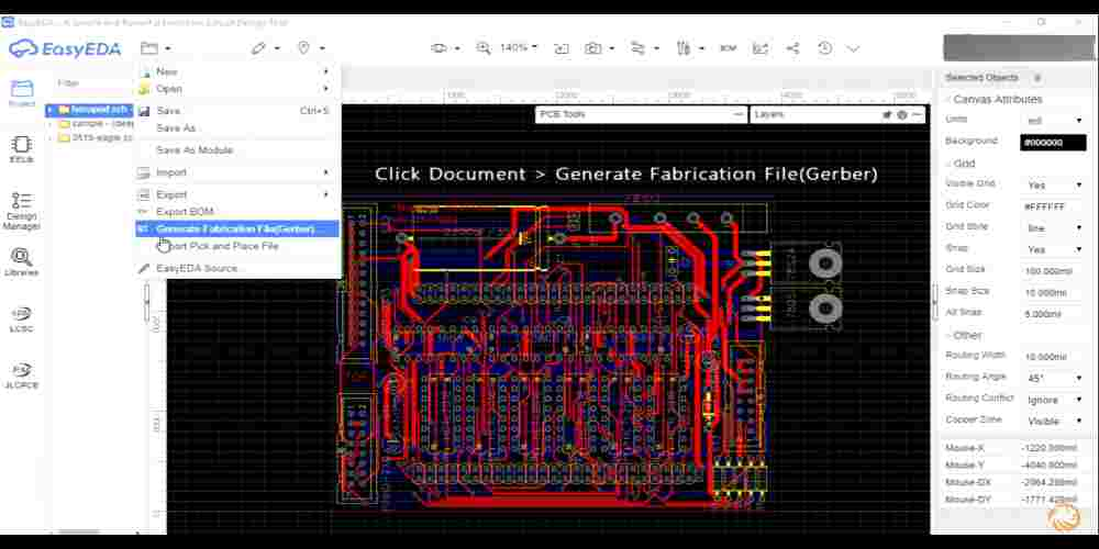
Exporting Gerber Files
To generate Gerber files from your KiCad PCB design, first, open the PCB layout editor. Then, go to the “Plot” option in the “File” menu. In the plot dialog box, select the layers that you want to include in your Gerber files. Make sure that you select all the necessary layers, such as copper, solder mask, and silk screen.
Next, specify the output directory and file name for your Gerber files. You can also choose to plot the drill files and add them to the same output directory. Make sure that you select the “Gerber” file format and that you choose the appropriate units for the output.
Once you have selected all the necessary options, click on the “Plot” button to generate your Gerber files.
Preparing Gerber Files for Manufacturing
After generating your Gerber files, you need to prepare them for manufacturing. This involves verifying that the files are correct and complete, and that they meet the requirements of your PCB manufacturer.
To verify your Gerber files, you can use a Gerber viewer tool to check that all the layers are present and that the design is correct. You should also check that the board outline and drill files are correct.
To ensure that your Gerber files meet the requirements of your manufacturer, you should check their specifications and guidelines. This may include checking the minimum trace width and spacing, the drill sizes, and the solder mask and silk screen clearances.
Once you have verified and prepared your Gerber files, you can send them to your manufacturer for production.
In conclusion, generating Gerber files from your KiCad PCB design is a straightforward process. By following the steps outlined above, you can ensure that your Gerber files are correct and complete, and that they meet the requirements of your manufacturer.
