Table of Contents
ToggleDDR4 memory is the latest standard in computer memory technology that has been widely adopted by the industry. It offers faster speeds, higher bandwidth, and lower power consumption compared to its predecessor, DDR3. However, achieving optimal performance from DDR4 memory requires careful consideration of the PCB layout.
The PCB layout of DDR4 memory plays a critical role in its performance. It determines the signal integrity, power delivery, and thermal management of the memory module. A well-designed PCB layout can help to minimize signal noise, reduce power losses, and improve thermal dissipation, which ultimately leads to better memory performance and stability. Therefore, understanding the principles of DDR4 PCB layout is essential for anyone involved in designing or troubleshooting DDR4 memory systems.

DDR4 PCB Layout Basics
When designing a DDR4 PCB layout, there are a few basics that should be kept in mind to ensure optimal performance. Two key considerations are signal integrity and power integrity.
Signal Integrity Considerations
Signal integrity is critical to DDR4 performance. Proper termination and routing of DDR4 signals can help to minimize signal reflections, ringing, and crosstalk. Here are a few key signal integrity considerations for DDR4 PCB layout:
- Termination – Proper termination is critical to minimizing signal reflections. Series termination is commonly used for DDR4 signals, with a resistor placed in series with the signal at the source. Parallel termination can also be used, with a resistor placed in parallel with the load. The value of the termination resistor should be carefully chosen to match the characteristic impedance of the transmission line.
- Routing – DDR4 signals should be routed as differential pairs to minimize crosstalk. The length of the differential pair should be matched to within a few mils to ensure proper timing. The differential pairs should also be routed with a controlled impedance, typically 50 ohms.
- Spacing – Proper spacing between DDR4 signals is important to minimize crosstalk. The spacing between differential pairs should be at least three times the width of the trace. The spacing between signals in the same differential pair should be at least twice the width of the trace.
Power Integrity Considerations
Power integrity is also critical to DDR4 performance. Proper decoupling and placement of power and ground planes can help to minimize noise and voltage drop. Here are a few key power integrity considerations for DDR4 PCB layout:
- Decoupling – Proper decoupling is critical to minimizing noise on the power supply rails. Decoupling capacitors should be placed as close as possible to the DDR4 devices, with a range of capacitance values to cover a broad frequency range.
- Placement – DDR4 devices should be placed as close as possible to the power and ground planes to minimize voltage drop. Power and ground planes should be placed adjacent to each other to minimize loop inductance.
- Routing – Power and ground traces should be routed as wide as possible to minimize resistance and voltage drop. Power and ground planes should be connected with multiple vias to minimize loop inductance.
By keeping these signal integrity and power integrity considerations in mind, designers can ensure optimal performance from their DDR4 PCB layouts.
DDR4 PCB Design Guidelines

When designing a DDR4 PCB layout, there are several guidelines that should be followed to ensure proper functionality and signal integrity. These guidelines can be broken down into three main categories: topology, routing, and termination.
Topology Guidelines
The topology of the DDR4 layout should be carefully considered to minimize signal reflections and crosstalk. The following guidelines should be followed:
- Place the memory controller and DDR4 memory chips as close together as possible to minimize trace length and reduce signal degradation.
- Place decoupling capacitors as close as possible to the power and ground pins of the DDR4 memory chips to minimize power supply noise and ground bounce.
- Use a star topology for the DDR4 memory chips, with each chip connected directly to the memory controller.
- Use a separate ground plane for the DDR4 memory chips to reduce crosstalk and improve signal integrity.
Routing Guidelines
The routing of the DDR4 signals is critical to ensure proper timing and signal integrity. The following guidelines should be followed:
- Use controlled impedance traces to ensure consistent signal performance.
- Route the address, command, and control signals first, followed by the data signals.
- Route the DDR4 signals in differential pairs to reduce crosstalk and improve signal integrity.
- Avoid routing DDR4 signals over split planes or through vias, as this can cause signal reflections and crosstalk.
- Keep the DDR4 signal traces as short as possible to minimize signal degradation.
Termination Guidelines
The termination of the DDR4 signals is critical to ensure proper signal integrity and timing. The following guidelines should be followed:
- Use series termination on the DDR4 data signals to reduce signal reflections and improve signal integrity.
- Use parallel termination on the DDR4 address, command, and control signals to reduce signal reflections and improve signal integrity.
- Use termination resistors that match the characteristic impedance of the DDR4 traces to ensure consistent signal performance.
By following these DDR4 PCB design guidelines, designers can ensure proper functionality and signal integrity of their DDR4 memory systems.
DDR4 PCB Layout Best Practices

When designing a DDR4 PCB layout, there are several best practices to follow to ensure optimal performance. The following sub-sections outline some of the critical factors to consider.
Component Placement
Component placement is crucial in DDR4 PCB layout design. Placing components too close together can cause signal interference, while placing them too far apart can lead to signal loss. Therefore, it’s essential to follow the manufacturer’s recommended placement guidelines.
To ensure proper signal integrity, it’s also recommended to place decoupling capacitors as close as possible to the power pins of the DDR4 memory chips.
Clock Routing
Clock routing is another critical factor to consider in DDR4 PCB layout design. Clock signals are highly sensitive to noise and can cause significant signal integrity issues if not routed correctly.
To minimize signal noise, it’s recommended to keep clock traces as short as possible and avoid crossing over other signal traces. It’s also recommended to use a dedicated clock layer and keep the clock trace width consistent throughout the design.
Memory Channel Routing
Routing the memory channels correctly is crucial in DDR4 PCB layout design. Improper routing can lead to signal reflections, crosstalk, and other signal integrity issues.
To ensure optimal signal integrity, it’s recommended to route each memory channel separately and avoid crossing over other signal traces. It’s also recommended to maintain consistent trace widths and lengths throughout the design.
In conclusion, following these best practices can help ensure optimal DDR4 PCB layout design. By carefully considering component placement, clock routing, and memory channel routing, designers can minimize signal noise and ensure optimal signal integrity for their DDR4 memory designs.
DDR4 PCB Layout Tools
When designing a DDR4 PCB layout, it is essential to use the right tools to ensure that the board meets the necessary specifications. There are two main categories of DDR4 PCB layout tools: simulation tools and layout tools.

Simulation Tools
Simulation tools are used to simulate the electrical behavior of the DDR4 memory interface and to verify that the PCB layout meets the required specifications. These tools are essential for identifying potential signal integrity issues and ensuring that the board design is optimized for performance. Some of the commonly used simulation tools for DDR4 PCB layout include:
- Hyperlynx
- Keysight ADS
- Cadence Sigrity
Layout Tools
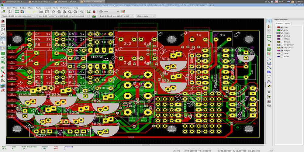
Layout tools are used to create the physical layout of the DDR4 PCB. These tools allow designers to place components, route traces, and ensure that the board meets the necessary mechanical and electrical requirements. Some of the commonly used layout tools for DDR4 PCB layout include:
When selecting DDR4 PCB layout tools, it is essential to consider the specific requirements of the project and to choose tools that are compatible with the design flow. It is also important to ensure that the tools are capable of meeting the necessary specifications and that they are easy to use and integrate into the design process.

