PCB assembly services are companies or individuals who can put PCBs together. These companies are sometimes called PCB assemblers or PCB manufacturers. PCB assembly is limited to assembling the components on the boards and involves other post-processing steps needed to get it ready for mass production.
Many factors affect the efficiency of the assembly process, such as the quality of raw materials used in making components, quality control standards, and corrosion standards. For example, the wrong type of solder paste might ruin the entire board, so hiring only the most qualified assembly companies is essential. One of these considerations is that they must be certified. They must also have experience working with different kinds of materials and components and compliance with industry standards.
There are many advantages associated with this kind of activity. These include meeting deadlines, avoiding errors, and avoiding risk management issues that sometimes cost more than anticipated.
Who can provide PCB assembly services?
PCB assembly is not only for large companies. Some small shops can often do these kinds of jobs with their own hands, but this method does not allow them to control the quality of the final product. The PCB assembly companies including can offer many other services. Most PCB manufacturers will provide assembly services in-house because it is cheaper and more flexible in customized designs.
Many PCB assemblers do not need to make the boards themselves, but they can still provide quality products once they receive the completed boards from manufacturers. Since you will most likely find some assembly services in this industry in China, it can be difficult for people to find reliable pcb assembly service providers. One of the key elements in finding a good PCB assembler is providing clients with documentation that certifies that the parts they assembled comply with the set specifications.
Many PCB manufacturers offer assembly services, but not all of them are good. Several manufacturers that offer the pcb assembly service usually do not provide any documentation to certify the quality of their work. Regardless of how cheap they might be, there is no point in dealing with companies like these because it may result in problems down the road.
The best PCB assemblers like RayMing PCB and Assembly provide certificates for each batch of boards that they assemble. Their certificates include certification of the final design, the details of the components used, and pictures or photographs of the final assembly.
Qualities that indicate whether a PCB assembler is good or not:
The PCBs market is growing fast, and the top five markets for PCBs are automotive, consumer electronics, telecommunications equipment, industrial equipment, and semiconductors. These markets accounted for about 57% of global shipments. Increased demand for smaller and more efficient PCBs will most likely drive PCB manufacturers to expand their manufacturing capabilities.
In addition, new partnerships between PCB manufacturers from different industries will help the industry grow. This collaboration will help consumers access a broader range of electronic products at a lower cost.
Various factors drive the market for PCBs, including price, product specifications, business models, and new technology.
Price:
The price of PCBs is significant because it can often determine how much of a product will sell. For example, if there are high-quality products that are not very expensive, they will likely be more popular than lower-quality products that are also not very expensive. Faster production lead times are also critical because it can be difficult to gain market share if the competitors are significantly faster. The average price of a single PCB set is $80. Some primary factors affecting the price of a PCB set are quantity, the board size, manufacturing method, and brand. The minimum price per board is $3 for 1-layer boards and $10 for 2-layer boards.
Product Specifications:
Product specifications determine how many products one can make with a particular PCB, essential for determining how popular it will be. For example, increasing the final product’s power output or storage capacity will likely increase its popularity. Manufacturers whose products have long lifecycles will benefit from this factor because they will still sell their products even after their competitors release newer models.
Business Models:
Some manufacturers have two separate divisions that develop different kinds of products. For example, one division might focus on laptops, and another will focus on desktop PCs. The market share of these companies is essential because it will affect the prices charged by their competitors for similar products.
New Technology:
New technology is also essential for the market’s growth to make products easier to build. For example, two firms may compete to develop products with greater processing power. As a result, they will likely use new PCBs that can handle more data in less time.
The different factors affect the PCB manufacturing industry
These include trends in the global economy, demand for PCBs in various industries, supply of materials used in making PCBs, and regulatory changes.
Global economy:
Changes in the global economy can affect the demand for finished PCBs. For example, when a country starts experiencing a recession, it might reduce the demand for electronics products because they are often luxury goods. The main exception to this is in industries such as the medical and telecommunications industry. Global economic crisis of 2008 is a prime example of how an economic downturn can lead to a decrease in demand for electronic components. The demand reduction led to many companies going out of business during this period.
Demand for PCBs:
The industry of application determines the demand for PCBs. For example, the demand for PCBs in the telecommunications industry was greater between 2008 and 2012 because of new technology such as cell phones. In addition, a growing number of people using mobile devices has increased the demand for these devices.
Supply of Materials:
Materials used in making PCBs can also affect the manufacturing process. For example, before the mid-1990s, most PCB manufacturers used materials such as ferrite and copper. However, some companies began to use copper foil in the 1990s because of its improved conductivity. This was important because it meant that PCB manufacturers could make smaller boards with higher power output.
Regulatory Changes:
Regulation changes for the production of PCBs are critical for their growth because these changes can lead to an increase in demand for these products among consumers or other industries. This is especially true in the electronics and telecommunications industries because regulation changes can significantly affect how companies produce and ship.
The price of a single PCB can vary greatly depending on how many boards you use and the manufacturing method employed. Numerous manufacturing methods used to produce a particular board also affects the cost of each board. For example, the price of a PCB that uses Double copper PCB technology will be 50% more than that of a single-sided board. Printing a silkscreen on a PCB will increase the price by at least 10%.
The manufacturers have to pay more for the ink they use to print their designs on each board. Insulating a PCB also increases its price. This is because manufacturers have to use more of their raw materials, which can be very expensive. In addition, there is a greater risk associated with insulating a PCB since machines may malfunction during this process and ruin an entire batch of PCBs.
There are many different manufacturing methods available for PCB manufacturers. For example, some PCB manufacturers use printing on both sides of the board while others only print on one side. This is important because it determines if each side of the board has an image or blank.
Other factors that affect the cost of a single PCB include: how many layers you will use to print on the board, how many times a particular design you will need to print, and the amount of space used for printing on each layer.
PCB manufacturing methods
We have are several methods for manufacturing PCBs. The most common process is called subtractive manufacturing, which is useful in removing only the board parts that are not useful. Some of the different subtractive methods available to PCB manufacturers include: manual, semi-automated, and fully automated.
Manual manufacturing
Manufactured PCBs are the most cost-effective because they require the least amount of resources to manufacture. However, they also take the longest to produce because each board has to be manufactured by hand. Most manual manufacturing processes involve an etching agent that can be harmful if inhaled. Manual manufacturing is typically helpful for prototypes.
Semi-automated manufacturing
We use semi-automated manufacturing for the production of simple PCBs that a software program designed. These programs are good in creating a detailed design for any PCB. In addition, the software is useful selecting the exact size and shape needed for each board.
Semi-automatic manufacturing requires a solder mask and etching agent to produce a finished board. Semi-automated manufacturing is very popular because it reduces the cost of PCB production. However, the semi-automatic method does not allow any fine adjustment to the design, so there is no guarantee that all parts will be correct.
Fully automated manufacturing
Fully automated manufacturing uses machines to manufacture PCBs without the need for human intervention. The machines rely on computer-assisted controls and automatic sensors to quickly produce a finished board with very few errors. Fully automated manufacturing is the most popular because it allows manufacturers to produce high quantities of PCBs quickly.
Challenges and impact of PCB manufacturing on the environment
The environmental aspects of PCB manufacturing are fundamental to consider because they can affect both the people that work at these facilities and the surrounding communities. These aspects focus on air pollution, water pollution, and waste disposal problems.
Air pollution
Sources of air pollution in PCB manufacturing facilities include chemical solvents, ionic copper solutions, inks used to print the designs, and the fabrication process itself.
We burn off the chemical solvents in a furnace when air pollution is measured. The UNEP reports that we can find small quantities of ozone-depleting substances (ODS) in PCB waste products. These substances can cause problems if we release them into the atmosphere.
Water pollution
Sources of water pollution in PCB manufacturing facilities include discharge of wastewater into lakes or rivers, effluent from the caustic soda recovery from the phosphoric acid cycle, and outflow from a sludge digester.
Effluent consists of wastewater sent to the sewer system, but it can also come from factories using or creating their sewer system. This fluid contains any used liquid waste from the manufacturing process. It can also contain chemicals that they will be using in the manufacturing processes.
The effluent discharged into rivers or lakes can change the chemical composition of these bodies of water. This can affect how life in these bodies thrives, including animals and plants.
PCB manufacturers must complete the United States Environmental Protection Agency’s National Pollutant Discharge Elimination System (NPDES) permit application. Additionally, the PCB manufacturers complete the United States Environmental Protection Agency’s National Pollutant Discharge Elimination System (NPDES) permit application. Applying for this permit requires an Environmental Engineer to ensure that all emissions are within allowable limits.
Waste disposal
A PCB manufacturer also has to deal with what it considers waste when creating printed circuit boards. We can reduce waste in this industry by using less hazardous materials. The waste stream produced in the PCB manufacturing process consists of solid, liquid, and gas waste.
Solid waste can come from many different places within the PCB manufacturing plant. This affluent waste usually comes through the use of machinery or manual labor. Solid waste can be reused or disposed of, but PCB manufacturers must follow common standards for proper disposal. PCB manufacturers that use a lot of solid waste should use a hazardous waste landfill.
Liquid PCB waste consists of any liquid that we get during the PCB manufacturing process. Some of this liquid may contain bio-hazardous or corrosive materials. These wastes usually require specialized treatment and disposal methods.
We consider gas waste hazardous when it results from a fire or an explosion in a PCB manufacturing plant. This type of waste usually has to be cleaned up by professionals, which can cause the use of large amounts of money and resources.
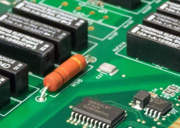
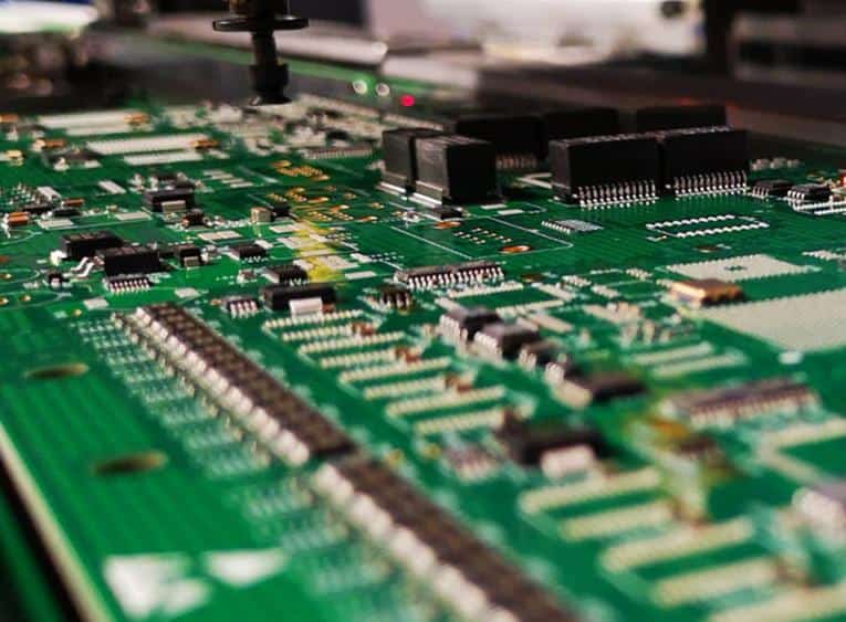
Process of PCB assembly

PCB assembly is the process of putting the individual components onto a printed circuit board. There are many different types of PCB assembly, but most factories use automated systems to do the job. Some processes are more complicated than others, but they all have similar steps that they go through.
Before the Assembly Process
A PCB’s construction begins with the component files (PCB Layout) coming from the manufacturer. One must review the files to ensure complete, clear, and accurate before being sent to the assembly process.
Designers or engineers most likely completes this step, but an assembler sometimes completes it due to human error on a dedicated design team.
The machines used for this review include scanners, digital cameras, and optical character recognition software.
Actual PCBA process steps
The actual assembly process is extremely complicated and can take hours or days to complete. While each step may seem simple, they are not always easy to understand. The process consists of numerous steps that are necessary for the finished product.
Step 1: Solder Paste Stenciling
Solder paste stenciling is the process of putting solder paste on copper surfaces that do not have components on them. It is a paste-like material that allows the application of solder to the parts in an even layer. This process is most commonly useful in surface mount soldering applications, but it is also evident in other soldering jobs.
Step 2: Pick and Place
Pick and place machines are useful in placing components onto PCBs during assembly. One can operate this machine manually, but a robotic arm usually controls it and automatically places the components into the appropriate holes. This decreasingly automated process allows low-volume PCB assembly to take place in a large factory.
Step 3: Soldering
The actual soldering process happens in a relatively small area between two areas or rooms where assembling and testing occur. This area is where we do most of this work, and it also has the most equipment and workers. We contain this area in a room defined by four walls with doors on either side. The soldering process requires soldering iron tips that are compatible specifically for each type of copper wire.
Step 4: Inspection and Quality Control
Once the PCB is complete, the first step is to inspect the circuit board for defects. The manufacturer does this by looking at each component, looking through it with a magnifying glass, and observing the spots where there was excess solder. If it finds defects, it can make corrections before going to test and QC. QC checks the finished product to make sure that it is as good as it can be.
Here is where we test the sample waveforms for each component to see how well they work together to function as a whole. The check the levels of each electronic component based on the factory’s standard of quality. If we find any discrepancies, then we will do another inspection before being shipped out to customers.
Step 5: Through-Hole Component Insertion
Through-hole components are different from surface-mount components because they require wires to be placed in holes before soldering occurs. The wire can be inserted manually or using a machine. To insert these parts, we have to open up the board to connect the leads to pre-drilled pads. We connect these leads by hand or with the help of a machine, depending on the component and manufacturer’s preference.
Step 6: Final Inspection and Functional Test
After the PCBA process is complete, the manufacturer must do a final inspection of the assembly. This helps to ensure that there are no defects in the final product. Manufacturers use many different machines and tools to find defects in boards, but they all have similar purposes. The ideal outcome of this process is to find no issues with any of the boards and get them shipped out to customers as soon as possible.
Step 7: Clean Up
The process produces many different types of waste. These wastes usually have to be disposed of appropriately to not get into the environment and cause problems for people and animals.
Step 8: Feedback
After the customer has received the product, the feedback process starts. The customer sends documentation about their bills to their manufacturer. You can do this can be done electronically or with paper documents. The customer can also send pictures of defects or any complaints that they have about the product.
Finding PCB assembly near me
Many factors go into finding the right place to have your PCBs made. Some of these factors include location, delivery, quality assurance, and cost. You only need to identify your needs and specifications for your desired PCB, then find the right company. There are many different places that you can have your PCBs assembled. Some of these places include local companies, global companies, and global contractors.
Local Companies: Some local companies hire independent PCB assemblers to take your PCBs and assemble them. These assemblers may not be as good as the ones that global companies use.
Global Companies: Global Construction Company take your PCBs and assemble them in an automated process. This process works best by using computers rather than humans to make the PCBs.
Global Contractors: Global Contractors are an option for people who need their sophisticated PCBs assembled. They also have rigorous quality checks and offer a swift turnaround.
Conclusion
PCB assembly has been a part of the electronics industry since its inception. It is a very complex and involved process that involves placing components onto a printed circuit board. We can break down the PCBA (Printed Circuit Board Assembly) process into six main steps mentioned in an electronic assembly plant article.
PCB assembly services offered by manufacturers can be very expensive, especially for large companies or businesses. The cost of the parts needed to make the boards is usually very low. Most PCBs do not use lead-free solder, but they still contain dangerous materials that you must dispose of properly. PCBs can be very useful in assembly because they are low-cost and offer maximum production efficiency. They also allow for more production in a short period, which is why we use them today. If a process is good, then you should use that good process in lower-manufacturing situations as well.
