Table of Contents
ToggleDouble-sided PCB design is a crucial aspect of modern electronics. These boards provide a more compact and efficient way to connect and integrate electronic components, making them essential for many applications. In this article, we will explore the basics of double-sided PCB design, including the benefits, challenges, and best practices.
Double-sided PCBs have two layers of conductive material, allowing for more complex circuitry and smaller board sizes. This design is particularly useful for high-density applications, such as smartphones, tablets, and other portable devices. However, double-sided PCB design also presents unique challenges, such as increased complexity, cost, and manufacturing difficulty. To overcome these challenges, designers must carefully consider factors such as signal integrity, power distribution, and thermal management.

What is Double Sided PCB Design?
Definition of Double Sided PCB Design
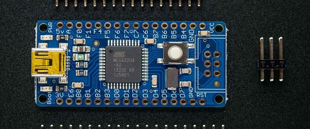
Double sided PCB design is a type of printed circuit board (PCB) that has conductive traces on both sides of the board. This means that components can be mounted on both sides of the board, increasing the density of the circuit and reducing the size of the board.
Double sided PCBs are also known as double layer PCBs. They are commonly used in electronic devices where a single layer PCB is not sufficient, but a multi-layer PCB is too complex or expensive.
Applications of Double Sided PCB Design
Double sided PCBs are used in a wide range of applications, including:
- Consumer electronics: Double sided PCBs are commonly used in smartphones, tablets, and other portable devices.
- Industrial equipment: Double sided PCBs are used in a variety of industrial equipment, including control systems, monitoring devices, and power supplies.
- Automotive electronics: Double sided PCBs are used in automotive electronics, including engine control units, navigation systems, and entertainment systems.
- Medical devices: Double sided PCBs are used in medical devices, including diagnostic equipment, monitoring devices, and implantable devices.
Double sided PCBs offer a number of advantages over single layer PCBs, including increased circuit density, reduced board size, and improved signal integrity. They are also more cost-effective than multi-layer PCBs, making them a popular choice for a wide range of applications.
Advantages of Double Sided PCB Design
Double sided PCB design is a popular choice for many electronic devices due to its numerous advantages. In this section, we will discuss the three main advantages of double sided PCB design: Increased Component Density, Improved Functionality, and Reduced Size and Weight.
Increased Component Density
One of the biggest advantages of double sided PCB design is the increased component density it allows. By using both sides of the board, designers can fit more components into a smaller space. This is particularly important for devices with limited space, such as mobile phones and wearables. By increasing the component density, designers can create more powerful and feature-rich devices without increasing their size.
Improved Functionality
Double sided PCB design also allows for improved functionality. By using both sides of the board, designers can create more complex circuits that can perform more functions. This is particularly important for devices that require multiple circuits to work together, such as audio equipment and medical devices. By using double sided PCB design, designers can create more sophisticated devices that can perform more complex tasks.
Reduced Size and Weight
Another advantage of double sided PCB design is the reduced size and weight it allows. By using both sides of the board, designers can create more compact devices that weigh less. This is particularly important for portable devices, such as laptops and tablets. By reducing the size and weight of these devices, designers can make them more portable and convenient to use.
In conclusion, double sided PCB design offers numerous advantages that make it a popular choice for many electronic devices. Its ability to increase component density, improve functionality, and reduce size and weight make it an ideal choice for devices that require high performance in a small package.
Disadvantages of Double Sided PCB Design

Higher Cost
One of the biggest disadvantages of double sided PCB design is the increased cost. Double sided PCBs require more materials and a more complex manufacturing process, which can significantly increase the cost of production. This is especially true for small production runs, where the cost per unit can be much higher than for larger runs.
More Complex Design Process
Designing a double sided PCB is more complex than designing a single sided PCB. The designer must take into account the placement of components on both sides of the board, as well as the routing of traces between the two sides. This can make the design process more time-consuming and require more expertise.
Increased Manufacturing Time
Double sided PCBs require a more complex manufacturing process than single sided PCBs. This can increase the manufacturing time, which can be a disadvantage for companies with tight production schedules. In addition, the increased complexity of the manufacturing process can lead to a higher rate of defects, which can further increase manufacturing time and costs.
In conclusion, while double sided PCBs offer certain advantages over single sided PCBs, such as increased circuit density and reduced board size, they also come with several disadvantages. These include higher cost, a more complex design process, and increased manufacturing time. Companies considering the use of double sided PCBs should carefully weigh these advantages and disadvantages before making a decision.
Design Considerations for Double Sided PCBs

When designing double sided PCBs, there are several key considerations that must be taken into account to ensure optimal performance and reliability. These considerations include component placement and routing, via placement and routing, and ground and power planes.
Component Placement and Routing
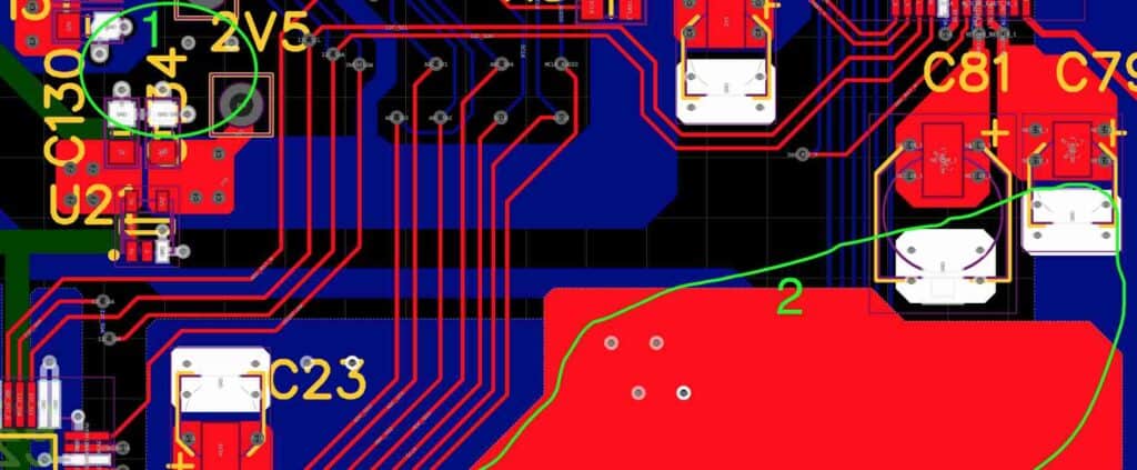
Careful consideration should be given to the placement of components on a double sided PCB. Components should be placed in a way that minimizes the length of their connections and reduces the likelihood of interference between neighboring components. Additionally, routing should be optimized to minimize the length of traces and ensure that they are as straight as possible.
Via Placement and Routing
Vias are an essential component of double sided PCB design, as they allow signals to pass between the two sides of the board. When placing vias, it is important to consider their size, placement, and routing. Vias should be placed in a way that minimizes their impact on the board’s overall layout, and their routing should be optimized to minimize signal loss and interference.
Ground and Power Planes
Ground and power planes are critical components of double sided PCB design, as they provide a stable reference voltage and help to reduce noise and interference. When designing ground and power planes, it is important to consider their placement and routing. Ground planes should be placed as close to the signal traces as possible, while power planes should be placed as close to the power supply as possible.
In summary, designing a double sided PCB requires careful consideration of component placement and routing, via placement and routing, and ground and power planes. By taking these factors into account, designers can ensure that their PCBs are optimized for performance and reliability.
Manufacturing Double Sided PCBs

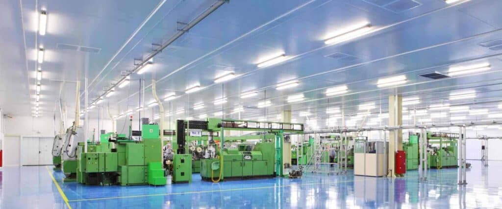
When it comes to designing and manufacturing double sided PCBs, there are several important steps that must be followed to ensure a successful outcome. In this section, we will discuss the key steps involved in the manufacturing process for double sided PCBs.
Drilling and Plating
The first step in manufacturing a double sided PCB is to drill holes in the board for component placement. Once the holes have been drilled, the board is plated with a thin layer of copper to create the necessary electrical connections between the two sides of the board. The plating process involves the use of a chemical solution that is applied to the board and then electroplated to create the required thickness of copper.
Solder Mask and Silk Screen Printing
After the drilling and plating process, the board is coated with a solder mask to protect the copper traces and pads from oxidation and other environmental factors. The solder mask is applied using a screen printing process that involves the use of a stencil to apply the mask material to the board. Once the solder mask has been applied, the board is silk screen printed with component labels and other identifying information.
Testing and Inspection
The final step in the manufacturing process for double sided PCBs is testing and inspection. This involves a comprehensive check of the board to ensure that all components are placed correctly and that there are no errors or defects in the board. Testing and inspection can be carried out using a range of techniques, including visual inspection, electrical testing, and automated optical inspection.
In conclusion, the manufacturing process for double sided PCBs involves several critical steps, including drilling and plating, solder mask and silk screen printing, and testing and inspection. By following these steps carefully and thoroughly, manufacturers can produce high-quality double sided PCBs that meet the needs of their customers.

