Table of Contents
ToggleElectronic PCB design is an essential component of modern technology. It involves designing and creating printed circuit boards that are used in a wide range of electronic devices, from smartphones to computers to medical equipment. PCB design is a crucial step in the process of creating electronic devices, and it requires specialized knowledge and expertise.
The design of a PCB involves laying out the various components of an electronic circuit on a board, and then connecting them using conductive pathways. This is done using specialized software that allows designers to create and test their designs before they are manufactured. PCB design is a complex process that requires a deep understanding of electronics, as well as the ability to work with specialized software and tools.
Overall, PCB design is an essential part of the process of creating modern electronic devices. It requires a combination of technical knowledge, design skills, and expertise with specialized software and tools. With the continued growth of the electronics industry, the demand for skilled PCB designers is likely to remain high in the years to come.

Basics of Electronic PCB Design
Understanding PCB Design Process
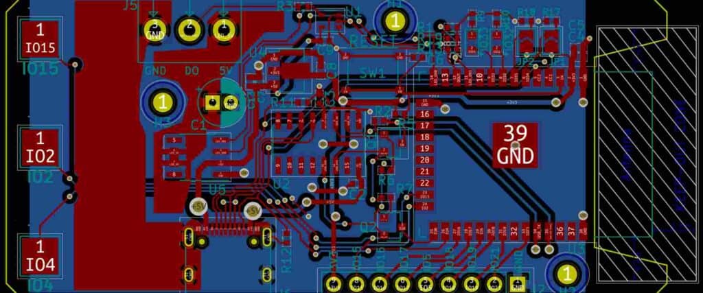
Electronic PCB design is a complex process that involves several stages. The process begins with schematic capture, where the circuit is drawn using a schematic editor. The schematic captures the electrical connections between the components of the circuit. The next stage is PCB layout design, where the physical layout of the circuit is designed. This stage involves placing components on the board, routing the traces, and ensuring that the design meets the electrical requirements.
PCB Design Tools
There are several PCB design tools available in the market, ranging from free to expensive. Some popular PCB design tools include Altium Designer, Eagle PCB, KiCAD, and OrCAD. These tools provide a range of features, including schematic capture, PCB layout design, and simulation.
PCB Design Rules
PCB design rules are a set of guidelines that define the minimum requirements for the design. These rules ensure that the design meets the electrical and mechanical requirements and can be manufactured without errors. Some common PCB design rules include trace width, clearance, and via size.
PCB Layout Design
PCB layout design is the process of arranging the components on the board and routing the traces. The layout design must consider the electrical requirements, mechanical constraints, and manufacturability. The layout design must also ensure that the board is compact and can fit into the enclosure.
In conclusion, electronic PCB design is a complex process that requires a deep understanding of the electrical and mechanical requirements. PCB design tools provide a range of features to simplify the design process, while PCB design rules ensure that the design meets the minimum requirements. PCB layout design is the most critical stage of the design process, and it must consider the electrical and mechanical requirements, manufacturability, and compactness.
Advanced PCB Design Techniques

High-Speed PCB Design Considerations
When designing a high-speed PCB, it is essential to take into account the signal integrity of the system. One of the critical factors to consider is the characteristic impedance of the transmission line. The characteristic impedance of the PCB trace should match the impedance of the source and load to prevent signal reflections.
Another important factor is the length of the trace. Longer traces can result in signal degradation, so it is best to keep them as short as possible. Additionally, it is crucial to avoid sharp corners, as they can cause signal reflections and distortions.
RF PCB Design Techniques
Designing an RF PCB requires special attention to detail. One of the critical factors to consider is the board’s layout. The layout should be optimized to minimize the length of the transmission lines and reduce the number of vias.
Another important factor is the selection of materials. The dielectric constant of the substrate material can significantly affect the performance of the RF circuit. Therefore, it is essential to choose a substrate material with a low dielectric constant to minimize signal loss.
Power Integrity in PCB Design
Power integrity is crucial in PCB design to ensure that the power supply voltage remains stable and does not fluctuate. One of the critical factors to consider is the decoupling capacitor placement. The decoupling capacitors should be placed as close to the power pins of the IC as possible to minimize the inductance of the power supply.
Another important factor is the power plane design. The power plane should be designed to minimize the impedance of the power supply. This can be achieved by using multiple power planes or adding a ground plane between the power planes.
In conclusion, advanced PCB design techniques require careful consideration of various factors, including signal integrity, layout, materials, decoupling capacitors, and power plane design. By implementing these techniques, designers can ensure that their PCBs perform optimally and meet the desired specifications.
PCB Fabrication and Assembly

PCB Manufacturing Process
PCB fabrication is a crucial step in the design process. The process involves creating the physical board that will hold all the electronic components. The manufacturing process consists of several steps, including:
-
Designing the PCB layout: This step involves designing the layout of the board using PCB design software. The software helps in creating the electrical connections between the components.
-
Printing the layout onto the copper board: Once the layout is complete, it is printed onto a copper board using a special printer. The copper board is then cleaned and prepared for etching.
-
Etching the board: The board is then etched using a chemical process to remove the copper from the areas that are not part of the design.
-
Drilling the holes: After the etching process, the board is drilled to create holes for the components.
-
Adding a solder mask: A solder mask is added to the board to protect the copper traces and prevent solder bridges.
-
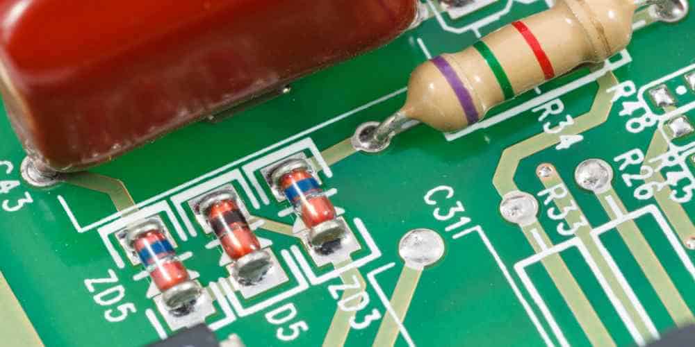
Adding a silkscreen: A silkscreen is added to the board to label the components and provide other important information.
PCB Assembly Process
PCB assembly is the process of attaching the electronic components to the board. The assembly process consists of several steps, including:
-
Solder paste application: Solder paste is applied to the board using a stencil. The paste is used to hold the components in place during soldering.
-
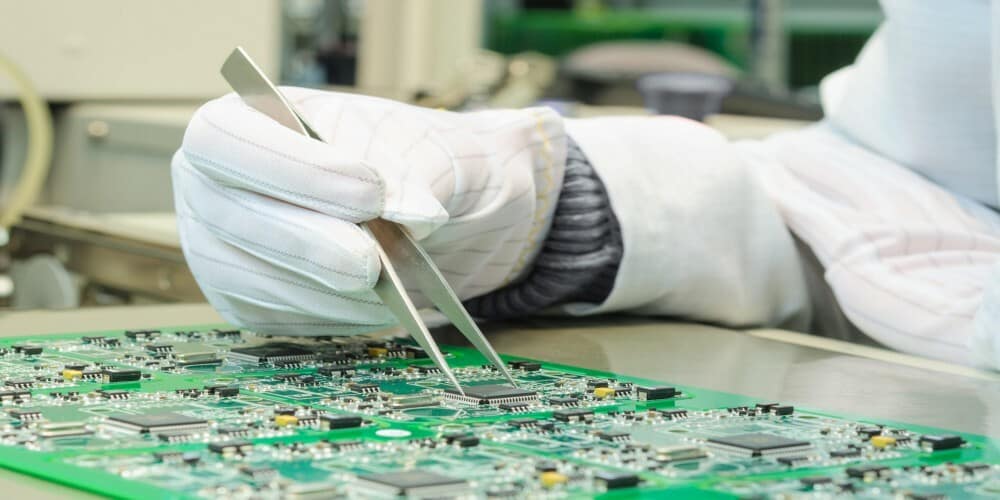
Component placement: The components are placed on the board using a pick-and-place machine. The machine picks up the components and places them in the correct location on the board.
-
Reflow soldering: The board is then placed in a reflow oven, where the solder paste is heated to melt and create a bond between the components and the board.
-
Inspection and testing: After the soldering process, the board is inspected and tested to ensure that all the components are properly attached and functioning correctly.
Overall, the PCB fabrication and assembly process is critical to the success of any electronic device. By following the proper procedures, designers can ensure that their boards are reliable and will perform as intended.
PCB Design for Manufacturing

When designing a printed circuit board (PCB), it is important to consider the manufacturing process. Designing for manufacturing (DFM) involves creating a PCB that can be easily and efficiently produced. This section will cover three aspects of DFM: Design for Assembly (DFA), Design for Test (DFT), and Design for Manufacturing (DFM).
Design for Assembly (DFA)
Design for Assembly (DFA) is the process of designing a PCB to make it easier to assemble. This can include using standardized components, minimizing the number of parts, and designing for automated assembly. By designing for assembly, the manufacturing process can be streamlined, reducing costs and improving quality.
Design for Test (DFT)
Design for Test (DFT) involves designing a PCB to make it easier to test. This can include adding test points, designing for in-circuit testing, and minimizing the number of test procedures. By designing for test, the PCB can be tested quickly and accurately, reducing the risk of defective products.
Design for Manufacturing (DFM)
Design for Manufacturing (DFM) is the process of designing a PCB to make it easier to manufacture. This can include designing for panelization, minimizing the number of process steps, and designing for manufacturability. By designing for manufacturing, the PCB can be produced quickly and efficiently, reducing costs and improving quality.
In conclusion, designing a PCB for manufacturing involves considering the entire manufacturing process, from assembly to testing to final production. By designing for assembly, test, and manufacturing, the PCB can be produced quickly, efficiently, and with high quality.

