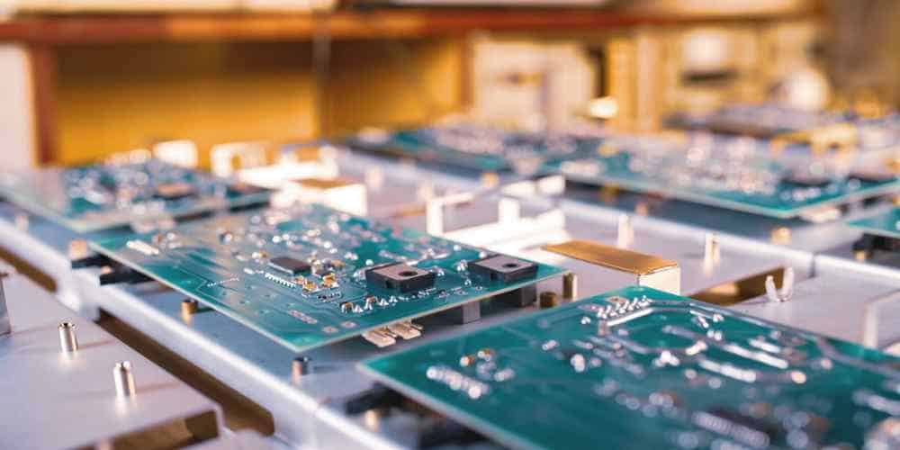
Printed Circuit Boards (PCBs) are designed in stages. At one stage, you are making the designs and at another, you are transferring that design to start the initial production. At other stages, you are testing the functional components of the board ahead of the final design and shipping.
While all these are sequential, as the completion of one stage opens up the door; it is also important to pay a special attention to the fabrication process. In this article, we explain most of the things you need to know about how a PCB is fabricated.
What is PCB Fabrication?
It refers to the process of creating or building the raw or bare board that serves as the foundation for the final Printed Circuit Board (PCB).
The transformation of the PCB design into the bare board is to be done in line with a variety of specifications. Following those to the latter helps to determine if the fabrication process will come out as expected.
PCB Design and Fabrication Process Checklist
For the best results, it is imperative to follow some of the checklists or list of important steps to take before fabricating a PCB.
These checklists do not only make the process simpler, but also intimates the PCB manufacturer on the expectations.
1. PCB Details
The first set of checklists to submit is the configuration and parameters for the Printed Circuit Board (PCB).
Working out these details with the manufacturer goes a long to add a boost to the layout of the design and the configuration of the physical circuit board.
Some of the parameters required here are:
- Circuit board panelization
- The stackups and configurations of the different layers in the PCB.
- Copper balancing
- Via types and structures
- Controlled impedance layers and;
- The minimum trace width and spacing
2. Completed Circuit Board Design
Once the PCB has been designed, it is subjected to another round of checks. This time, the following parameters will help you determine if the PCB’s design is complete or not:
- BOM Review: the Bill of Materials (BOM) must be reviewed. The review helps in finding out the available components on the board.
- Engineering Review: the PCB must have been put through a full engineering review.
- DFM Compliance: the rules for the Design for Manufacturing (DFM) must have been reviewed. The outcome of the review should certify that the circuitry is error-free and due for assembly of the components.
- Schematic Synchronization: the layout and schematic databases are to be updated and synchronized.
- Design Rule Checks: all the design rules and constraints for the PCB must be checked. If there are errors noticed, they are to be corrected or fixed.
- Routing: all of the components required for the PCBA are to be placed on the board and all the net connections are to be routed, accordingly.
- The other checklist is the completion of the following: power integrity analysis, circuit simulation and signal integrity.
3. Circuit Board Manufacturing Data
The completion of the earlier two stages paves the way for the provision of the data needed for the PCB manufacturing process.
A full set of fabrication and assembly data files is to be generated and submitted to the PCB manufacturer for the final circuit board design.
Examples of the files required here are:
- Netlist
- Bill of Materials (BOM)
- Test point locations
- Pick-and-place or component XY locations
- Schematic
- Formatted board layer image files, such as the Gerber files and;
- The manufacturing drawings for the fabrication and assembly of the PCB.
The PCB Development Stages at a Glance

The fabrication of a PCB is not even the first step. It is the second and there are a couple of other sequences that come after it.
Here is a summary of the different steps that come together to facilitate the production of Printed Circuit Boards (PCBs):
1. Circuit Board Design
The first step is to make a design of the board. You can use a PCB software to come up with this schematic.
2. Circuit Board Manufacturing Process
This is a two-way process that involves the fabrication and assembly of the board. First, the fabrication has to do with the transfer of the schematic to the bare board to serve as the foundation for the PCB to be designed.
The completion of the PCB fabrication process leads to the next stage – PCBA. With the full name as Printed Circuit Board Assembly (PCBA), it refers to the placement or mounting of the electronic components where they are designated to be on the PCB’s surface.
3. Circuit Board Testing
Before a PCB is shipped, its functional components are tested to be certain of the performance. As the third stage of the circuit board development process, the testing period helps the PCB manufacturer to discover some of the flaws or design errors.
The early detection of these faults helps the designer/manufacturer to fix the issues to avoid triggering unexpected problems when the PCB is coupled for use.
4. PCBA
As one of the most important stages in PCB board fabrication process, the PCBA process refers to the assembly of the components on the board’s surface.
The assembly can either be done via soldering these electronic components or mounting/placing them on the designated points on the PCB’s surface.
The PCB Fabrication Process Steps
Here are some of the steps involved in fabricating a Printed Circuit Board (PCB):
1. Desired Layout Imaging
This refers to the imaging or recognition of the areas or surfaces that would later become the medium for inserting the metal ground, traces and pads for the PCB.
The Laser Direct Imaging (LDI) process is used here to image the desired layouts on the copper clad laminates. The processes to doing this are:
- Applying a dry film to the copper laminate.
- Using the Laser Direct Imaging (LDI), certain parts of the PCB will be exposed to light in the shape of the circuit board’s pattern.
2. Excess Copper Removal
The process of removing excessive copper from the PCB’s inner layers is called etching. The etching or removal process helps to reveal the pads and traces on the PCB.
Here are the steps involved for etching a PCB’s surface:
- The unexposed PCB parts will be removed or etched off. In addition to revealing the pads and traces, the process also leaves behind a dry film that acts as the etch barrier.
- The etch barrier is also used to form the copper circuitry.
3. PCB Sandwiching
This process is generally called lamination. It has to do with the creation of the circuit board’s layer stackup by way of heating and pressing of the board materials at higher temperatures.
The following steps underscore the PCB lamination process:
- A chemical treatment called oxide is applied to the PCB’s inner layers. This should help in strengthening the connection or bond of the inner layers.
- The second step is to use a combination of heat and hydraulic pressing to join, sandwich or combine the copper foil and prepreg PCB materials.
4. Hole Drilling
Holes are to be drilled as a way of facilitating signal transmission. Note that the drilled holes work best for the multilayer PCB fabrication process, which enables the transmission or sending of signals from one layer to the other.
The following considerations are to be made:
- A stack of 2 to 3 panels can be used to drill the holes. Of course, this depends on the type of vias being used.
- Copper will then be used to plait the holes. Doing so enables the electroless copper deposition – a medium for sending electrical signals from one layer to the other.
5. Metallic Base Creation
The next step is the creation of the metallic base for the electroplating process. The steps to achieving this include:
- The usage of mechanical and chemical processes to remove excess debris and resin from the PCB’s surface.
- A thin coating of copper will then be deposited or placed on all of the exposed parts on the PCB’s surface/panel.
- Dry film can now be added to the outer layers of the copper panel.
- Expose the dry film to Laser Direct Imaging (LDI) to produce a conductive pattern.
6. The Electroplating Process
The electroplating process requires the immersion or placement of the PCB panel into a copper plating bath. The copper sulfate and sulfuric acid are commonly used to form this bath/solution.
The following are the steps involved in electroplating a PCB’s panel:
- After immersing the panel into the bath, make sure to add electrical current.
- The next step is to deposit copper onto the PCB board’s conductive surface. A thickness of 1 mil should be used.
- Remove the plate from the bath and have it placed into a tin plating bath. This makes it serve as an etch barrier.
- Remove the dry film so that the exposed copper, which is not covered by the tin plating bath, will be removed/etched away.
- The completion of the etching process reveals the pads, traces and other patterns on the plate.
- The final step in this stage is make a chemical stripping of the tin plating. This leaves copper only in the precise areas it is needed.
5. Protect the PCB’s Surface
The circuit board’s surface needs to be protected with a protective coating. The option here is to add a solder mask.
Here is how to go about it:
- Apply the solder mask on the PCB’s surface. It is a thin layer of polymer that protects the PCB’s copper traces from oxidation. Solder mask also helps to prevent unintentional connections (solder bridges) from forming between two conductors on the PCB.
- The solder mask has to be applied with a similar Ultraviolet (UV) light exposure using during the photoresist stage.
6. Apply Silkscreen to the PCB
Silkscreen is a process of integrating or imprinting the different references required for a PCB. Examples of these references are:
- Logos
- Component reference designators and;
- Polarity indicators
After the application, make sure to cure or treat the silkscreen and solder mask by baking the PCB in an oven, at the recommended temperature.
7. Apply a Surface Finish
A surface finish is used to further enhance the protection of the PCB. It is often added to the exposed metal surfaces that were not covered by the solder mask ink.
The surface finish helps to smoothening the soldering process, as well as protecting the exposed metal surfaces in the PCB.
8. Verify the Functionality of the PCB
The completion of the above steps helps to enhance the performance of the PCB board. Just to be sure, you got to subject the circuit board to a series of tests and inspections to be certain of the functionality.
You may also want to ask the PCB manufacturer to use automated pieces of test equipment to streamline the process and to validate the functionality of the PCB.
Differentiating between PCB Fab and Assembly
PCB fabrication and assembly are two different concepts, but they come under the umbrella for developing a circuit board.
While the fabrication has to do with the transfer of the design into the bare board for laying the PCB’s foundation; the assembly has to do with the placement or insertion of the electronic components. The fabrication process is completed before the assembly process.
Conclusion: Find a Reliable PCB Fab House
While the concept of the circuit board’s design lies with your imagination and your needs; a bulk of the job is handled by the PCB manufacturer. Thus, choosing the right contract manufacturer with a mastery of the different PCB fabrication methods is a plus.
As a Contract Manufacturer (CM), Hillman Curtis helps you translate the schematics or designs into the bare board, assemble or arrange the components on the board and inspect the same before shipping.
Our extended list of verified vendors is also a bonus, as we source the components required for the assembly in real-time. From the creation of the bare boards, the fabrication of the same and the use of specific materials, such as FR-4, we take pride in offering all the services, in-house.
Why not contact us today to help translate the designs you have conceptualized into a working Printed Circuit Board (PCB)?
