The field of electronics is complex, and there are various phenomena taking place in this field. Using acronyms and abbreviations, especially three-letter ones, can cause problems for professionals and students in the field because they can confuse them.
PWBs are similar to PCBs and are commonly used in designing and manufacturing electronic products. Therefore, it is important to know the disparity between the two.
This article will look at wiring assembly on PCBs, which is our focus. Next, we will discuss the main factors that affect the operation of a printed circuit board.
What is a Printed Wiring Assembly?
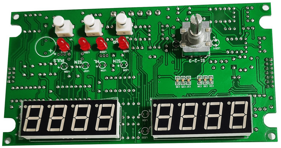
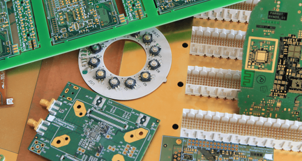
After soldering the electronic components, the board is called a PCB assembly (PCA), printed circuit board assembly (PCBA), or Printed circuit board assembly. Printed circuit boards are known as PCBs before the electronic components are assembled. Various manual and automatic PCB assembly tools are used in this process.
It should be noted that PCB assembly differs from the PCB manufacturing process. PCB manufacturing involves several processes, including PCB design and PCB prototyping. Once the circuit board is complete, the active and passive electronic components must be soldered before they can be used in any electronic equipment or gadget. The installation of these electronic components depends on the type of circuit board, the type of electronic component, and the purpose of the circuit board.
What is a Printed Wiring Design?
Like other major components, printed circuit boards are very important to all electronic devices. They were introduced back then in the early 1950s. They serve as the building blocks of all electronic packages.
An important characteristic of printed wiring boards is to get the most components per square inch of the printed wiring board (PWB). We call this component density. This has resulted in several packaging methods. In addition, the surface mount components are small in size. It is also widely used in most printed circuit boards. This allows for maximum component density while maintaining some degree of thermal, electrical, and signal integrity.
There are also various useful materials for PCB substrates. It should be noted that FR4 is most often used.
What Are the Main Factors Affecting the Performance of Printed Circuit Boards?
Circuit board operation may be affected. The following are the main factors:
1. The Speed of Operation of the Printed Circuit Board
An important factor in PCB interconnect design is the operating speed of electronic devices. It must be very short of ensuring that the system’s electrical performance is optimal. Furthermore, the proportional speed of the signal is inversely proportional to the Dk (dielectric constant) of the substrate material of the PCB. In addition, the time of flight is known as the signal’s propagation time, which is directly proportional to the length of the conductor.
2. Power Consumption of the Printed Circuit Board

Increasing the number of gates and the clock frequency will increase power consumption. You have to be careful with high-speed switching circuits where the flow of current back to the ground is optimally diverted. In addition, the multilayer printed circuit board (PWB) must have a separate or distinct ground plane. It is primarily designed to allow low-resistance current flow. In addition, a different bus system is required. In addition, it is better suited for heavy-duty circuits.
3. Heat Management
Printed circuits are poor conductors of heat. Therefore, you must be careful when using a method to remove the heat generated by the power consumption of the circuit board. Metal balls, conductive planes, thermal holes, and heat sink circuit boards are great techniques.
Things Needed For Circuit Board Assembly
After PCB assembly, tools, electronic parts, and consumables are required for PCB assembly:
- Circuit board
- Basic electronic components
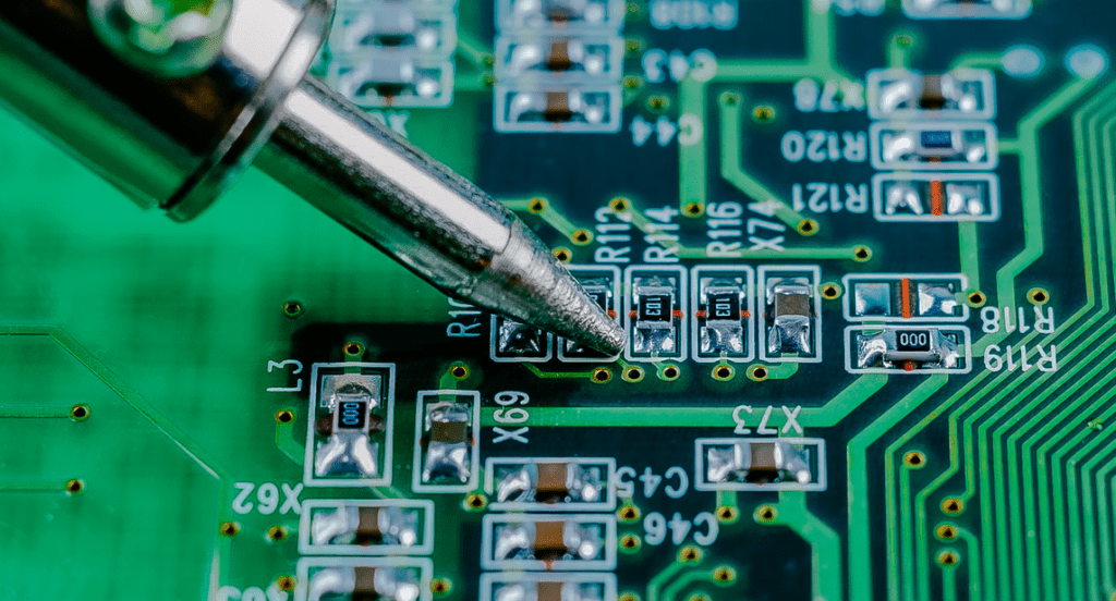
- Soldering materials include solder wire, solder pastes, solder rods, solder balls for BGA, and solder blanks.
- Soldering flux
- Soldering equipment, including soldering station, wave soldering equipment, SMT equipment, inspection, testing equipment, etc.
Once all the above equipment, electronic parts, and all raw materials are in order, it’s time to start the circuit board assembly process.
PWB vs. PCB: What’s the Difference?
The difference between a printed circuit board and a printed circuit board is explained below:
● Ingredients
When comparing printed wiring boards and printed circuit boards, one of the most obvious and important differences is that the printed circuit board (PCB) is the board that contains all the circuits. However, printed wiring boards are associated with component-free boards. In addition, PWB helps demonstrate basic printed circuit board manufacturing. It also demonstrates PCBs in electronics that do not require complex functions.
● Area and Location
The term used at the time was printed circuit board. It was a time when the world of electronics was still in its infancy. Throughout the early days of the industry, printed wiring board was considered a proper noun or term because the connections found on the board were mostly one-to-one. Also, due to great technological advancement, PCBs have reached a wide population with limited printed wiring boards (PWBs) for pre-production electronics.
Process of a Soldering PCB Assembly
- Insertion of electronic components
- Streaming request
- Heat up
- Wave soldering
- Cleaning
- Testing
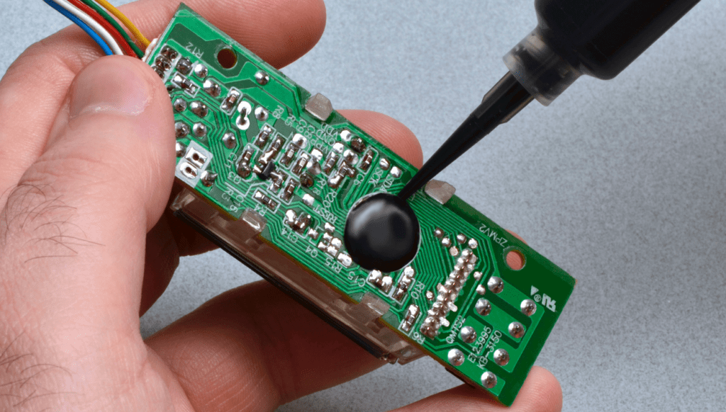
After wave soldering is complete, the PCBA is cleaned and inspected. If defects in the solder joints are found, such as pinholes or shock wave soldering defects, they are sent for rework, usually done by hand.
Manual welding is performed in production plants with lower workloads or processing/repair works. This process uses a good quality soldering station or soldering iron and wire and solder flux.
Factors That Can Affect PWB Performance
The final product’s performance depends on the construction quality of the PWB. There are many factors that PCB designers and assemblers must consider when designing printed wiring boards for their PCBs. It includes:
1. Speed of Operation
In the final product, the circuit on the PWB will send current from the power source along the traces to the components and then back. This is mainly due to the copper effect built into the board; the surrounding substrate affects signal strength and speed.
Substrates harm the signal’s propagation time, called the time of flight. Mathematically, it is inversely relative to the square root of the dielectric constant of the substrate matter. The thicker and less conductive it is, the higher the signal impedance.
2. Use of Power
Power consumption is a constant problem when building a printed circuit board assembly, and problems can start as early as the PWB stage. As the number of circuit gates increases, so does the power consumption. When designing the PWB, the ideal power supply should be considered, and the number of gates and clock frequencies should be adjusted accordingly.
3. Deadline Management
The PWB itself conducts heat inefficiently. The substrate absorbs and stores heat, so you need to include another method on the PWB to dissipate the heat build-up.
While FR4 is the best choice for most circuits as it can absorb a good amount of heat, faster ones require more heat-handling capabilities.
How Are PWBs Made?
You discover that circuit boards are made from various manufacturing processes. This process includes any other materials and equipment you deem essential to the success of the process.
Completing the PWB will include the following steps:
● Lamination
To form a laminate, the lamination process combines substrate layers and prepregs under heat and pressure. The substrate is usually a dielectric material such as FR-4 or ceramic that provides electrical isolation of the conductive layer.
● Ceramic circuit board
On the other hand, prepregs are resin-based formulations used to hold laminated parts together. During the lamination process, it is found that the substrate and the prepreg layer are glued together.
They are then consolidated in a press and placed in a controlled oven where the heat melts the prepreg. The temperature is high enough to soften the prepreg without running. This allows it to adhere firmly to the surface of the substrate when it hardens.
● Drilling
The purpose of the drilling process is to drill holes to install components and holes. You find that drilling is done on individual layers of laminate, and if multiple layers are involved, a different lamination procedure will follow.
Drilling can be done manually and automatically using a variety of machines and equipment. Laminate or guide plates are usually marked for holes.
● Formation of the leading path
Conductive traces are an important feature of a circuit board. The standard material used for conductive rails is copper due to its signal transmission quality and availability. You find that this track provides the desired electrical signal path.
There are two approaches to creating lead traces: additive and subtractive.
The additive method involves depositing copper onto the surface of the substrate in the desired manner. Instead, you can find a push approach to use an etched copper film to remove unwanted material. The desired model of the shape of the conductive path is then obtained.
What Affects the Current Carrying Capacity of the PWB?
A printed circuit board provides a path for the transmission of electrical signals when used as a PCB. You may find PWBs with different current carrying capacities affected by various factors. Some important factors include the following:
● Field of Application
Printed circuits are used in many areas, such as electronics, heavy industry, automotive, and aerospace applications. Current operator requirements vary from application to application.
● Copper Thickness
Copper weight (ounces) describes the thickness of copper when placed evenly on a flat surface, one square foot. The copper thickness on a PWB is determined by the weight of copper used in manufacturing. The greater the thickness of the copper used, the greater the current carrying capacity of the PWB.
What Factors Determine Printed Circuit Board Assembly Design?
Printed wiring design is not as easy as electronics production. Pay attention to point-to-point connection on bare boards and ensure the entire circuitry aligns on the single-sided boards. Every component attached should also be adequately labeled. From the surface mount and laser drilling, anyone can understand the insulating material needed for the etching solution. The design of a printed circuit board depends on several factors, including:
● Application domain
PWBs are used in various industries for unique functions like solder paste and point-to-point connection. You need to determine the needs of your application and incorporate them into your design. A key consideration for an application domain PWB is the current requirement. This information is necessary to determine the thickness of the copper.
● Costs
Estimating costs is important for any design project, especially when there are budget concerns. PWB costs will increase with the complexity of the inner layers, electrical conductivity, integrated circuit, thin layer, and unwanted copper, and the circuit card assembly to be used. For example, a multilayer card configuration will cost more than a single-sided card. Other factors to consider when deciding the costs include a conductive material, conductive tracks, and consumer electronics attached to it.
● Configuration
Table configuration is a design element that defines how the table of multilayer boards will be structured and the through-hole components that will be included. The panel’s overall thickness will affect the panel’s configuration, conductive tracks, and area of use. There are several different card configurations to choose from. You will find single-sided cards, double-sided cards, and multi-layered cards.
● Density of Components
Printed wiring boards are designed to provide electrical connections for circuits connected to perform a specific function which could be physical and chemical processes. When designing a board, you need to know the number and type of components to add. This information can help you create an appropriate layer structure.
● Heat Requirements
Printed circuit assembly can be used in applications with high heat dissipation. It is important to include thermal design elements in the design of the card to ensure that there is no heat build-up. If left unchecked, you find that heat build-up can damage the board by causing stress.
What Are Some Advantages of Choosing the Right Printed Wiring Board?
There is no denying that PWB has many advantages. It is ideal for companies that manufacture various electronic equipment, devices, and components. Now let’s explain some of the main advantages of the printed circuit assembly.
● Compact Size
Many small components can fit into one simple PCB. Instead of using standard wires, copper traces are used to connect these components. As a result, hundreds of components can be connected without worrying about PCB size. This compactness creates complex electronic circuits without taking up much space.
● Easy to Diagnose and Repair
With PCB, you can quickly diagnose and solve problems. The board is made with labels indicating the polarity of the electronic components. Easy to check for problems and make replacements. In addition, the PCB makes installation easier. It is often easier to trace the signal path during diagnostic procedures.
● Saves Time
When it comes to connecting components, classic boards take a lot of time. Therefore, if you need to assemble a circuit quickly, the PCB takes less time.
● Lack of Movement
All PCB components are attached to the board using solder flux. So the components won’t move no matter how much you move the board. As a result, the chain is much safer for everyday use.
● A Strong Connection
You won’t find any shorts or loose connections because the connections are made through copper traces and other electrical components on the surface mount technology of the printed wire boards used for electronics manufacturing. A strong connection must be created on the printed wire board while ensuring there are conductive layers for PCB fabrication along the desired copper pattern without any bare copper traces.
● Electronic Noise Reduction
If the components are arranged carefully enough, the PCB can help reduce electronic noise. However, circuit board performance can be affected by noise if the layout needs to be done correctly, especially when it is term printed wiring boards for an electronic circuit. In addition, circuit boards contribute to the emission of electronic noise from heat, radiation, and flicker.
● Lower Price
Because PWBs are inexpensive, they allow the production of large numbers of printed circuit boards without incurring large costs. One of the major things to consider when it comes to PWB vs. PCB is the low cost of PWB connect electronic components on the board surface.
● Increased Reliability
Thanks to all the above advantages, a term printed wiring board is more reliable than conventional boards because of the automated optical inspection. With a printed wiring board, you can have as much printed wiring on the printed wiring board. Not only are you guaranteed reliability for the copper layers and point-to-point connection, but other consumer electronics are also reliable.
Conclusion
This is the end of our article on printed circuit boards. We can explain what it is. We also explain how it differs from a printed circuit board. If you need clarification on any aspect of the article, don’t hesitate to ask your question. We have specialists in this field ready to help you, and from the record of quality, Hilman Curtis appears to be the best. When you contact them today, you can be sure to get the best-printed wiring assembly where everything is well-fitted.
