The landscape of printed circuit board (PCB) design has been consistently evolving to keep up with the relentless advancement of electronic devices. As components become smaller and more powerful, the demand for high-density interconnect (HDI) PCBs has risen to accommodate intricate designs and meet performance requirements. HDI PCBs utilize advanced manufacturing techniques to enable more components and connections to fit into a smaller space, without compromising the overall functionality and reliability of the board.
Designing an HDI PCB that is most suitable for your needs can be a complex task, requiring careful consideration of various factors such as component selection, materials, and layout strategies. By understanding the fundamental principles of HDI technology and incorporating best practices in your design process, you can achieve a tailor-made solution that effectively meets your requirements while maximizing performance.
To embark on your HDI PCB design journey, it is crucial to familiarize yourself with the available design tools, material options, and manufacturing limitations. Ensuring a comprehensive approach to the design process will not only minimize potential issues but also pave the way for the creation of a high-performing and reliable HDI PCB. Remember that every design is unique and requires attention to detail to achieve the perfect balance between functionality, size, and cost.
Understanding
HDI PCB Design Process
Schematic Capture
In the HDI PCB design process, the first step is schematic capture. This involves translating the design concept into an electronic format, which serves as the blueprint for the entire design. During schematic capture, components are selected and placed on a virtual workspace, with connections and nets being defined to create a functional representation of the circuit:
- Choose components from a library
- Define connections and nets
- Label and annotate components
This stage is critical to the eventual performance and functionality of the PCB, so it is essential to carefully review and verify the schematic before moving on to the next step.
Layout Design
Once the schematic has been captured and verified, the next step in the HDI PCB design process is layout design. This involves arranging the components from the schematic onto a physical board, while optimizing for space, performance, and manufacturability:
- Optimize component placement for performance
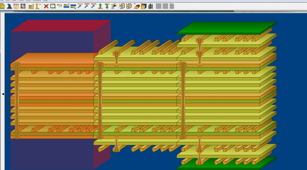
- Route traces between components, using HDI-specific techniques such as blind vias, buried vias, and microvias
- Consider thermal, mechanical, and electromagnetic aspects
During the layout process, designers need to carefully balance considerations such as signal integrity, power distribution, and EMI/EMC, while using the advanced features of HDI technology to create a compact, high-performance design.
Design Rules Check
Once the layout has been finalized, the HDI PCB design must undergo a crucial step called the design rules check (DRC). The DRC verifies that the design complies with the manufacturer’s specifications and guidelines, helping to avoid costly issues such as fabrication errors or performance issues:
- Check trace widths, clearances, and via sizes
- Verify component clearances and orientations
- Confirm manufacturing tolerances and requirements
By thoroughly checking the design against the rules and guidelines, the chances of encountering issues during the manufacturing process are significantly reduced, leading to a more successful outcome in terms of both performance and cost.
Selecting Materials and Components
When designing an HDI PCB, it’s essential to choose the proper materials and components to meet your specific requirements. In this section, we’ll discuss the importance of selecting the right PCB substrate and surface finish options.
PCB Substrate
The PCB substrate serves as the foundation of your design and directly impacts the overall performance of your board. Several factors to consider when selecting a substrate material include:
- Electrical properties: Choose a substrate with appropriate dielectric properties for your application.
- Thermal properties: Ensure the material can withstand the heat generated by the PCB during operation.
- Mechanical properties: Consider the material’s rigidity, weight, and thickness that best suit your design requirements.
Some common PCB substrates include:
- FR-4: A widely used material with good electrical and mechanical properties, offering a balance between cost and performance.
- Polyimide: A high-performance material known for its excellent thermal stability and mechanical flexibility.
- Rogers: A high-frequency substrate with outstanding electrical properties, often used in advanced applications such as aerospace and telecommunications.
Surface Finish Options
Selecting the right surface finish is crucial for enhancing the solderability and longevity of your HDI PCB. There are several surface finishes to choose from, and the best option depends on your application and budget.
Some popular surface finish options include:
- HASL (Hot Air Solder Leveling): A cost-effective option providing good solderability and shelf life, but not well-suited for fine-pitch components.
- ENIG (Electroless Nickel Immersion Gold): A high-quality finish offering excellent solderability and corrosion resistance, but has higher cost.
- OSP (Organic Solderability Preservative): A thin layer of organic film offering good solderability and lower cost, but has a shorter shelf life.
When selecting materials and components for your HDI PCB design, carefully consider the factors mentioned above to achieve the optimal balance between performance, durability, and cost.
Miniaturization and Signal Integrity

As technology advances, the demand for smaller and more compact devices continues to grow. This push for miniaturization in HDI PCB design presents a set of unique challenges that must be carefully considered to ensure optimal performance and reliability of the final product.
Trace Width and Spacing
One of the primary concerns when designing an HDI PCB with miniaturization in mind is the trace width and spacing. As components and packages continue to shrink, the need for narrower traces and tighter spacing is essential to maintain signal integrity. Here are a few key factors to take into consideration:
- Trace width: As the trace width decreases, the current carrying capacity reduces, potentially leading to overheating and compromised performance if not accounted for during the design phase.
- Spacing: Reducing the spacing between traces increases the risk of crosstalk, as signals from different nets may create interference.
- Manufacturing limitations: It is crucial to be aware of the manufacturer’s capabilities and limitations when determining trace width and spacing, ensuring the design can be accurately produced.
Impedance Control
Another crucial aspect of HDI PCB design related to miniaturization and signal integrity is impedance control. In high-speed digital signals, maintaining a controlled impedance environment is necessary to prevent signal distortion and reflection, which could lead to data corruption and loss. Some key points to consider when designing for impedance control include:
- Characteristic impedance: Calculate the target impedance by accounting for the dielectric constant, trace width, thickness, and distance from the reference plane.
- Material selection: The dielectric material and its properties play a significant role in the impedance control process. Material of the PCB should be carefully chosen to match the desired impedance.
- Layout considerations: Properly routing the traces, utilizing ground planes, and carefully managing the spacings and layers will help to maintain the desired impedance throughout the design.
In conclusion, ensuring miniaturization and signal integrity in HDI PCB design involves careful planning and consideration of trace width and spacing, as well as impedance control. By paying attention to these critical aspects, designers can create PCBs that are compact, efficient, and meet the requirements of today’s high-tech devices.
Thermal Management
Heat Dissipation Techniques
Effective thermal management is crucial in HDI PCB design to prevent component overheating and ensure optimal performance. One common strategy is the use of heat dissipation techniques to keep the board’s temperature within safe limits. Here are some popular heat dissipation techniques:
-
Heat sinks: These are metal structures placed on heat-generating components to absorb and disperse heat away from them. Heat sinks are available in various shapes and sizes to accommodate different component requirements.
-
Conductive planes: Using copper planes for power and ground layers can help distribute excess heat across the PCB, minimizing thermal stress on critical components.
-
Proper component placement: Placing heat-generating components in areas where airflow is relatively higher or strategically spreading them across the board can help distribute the overall thermal load.
Thermal Vias
Another critical aspect of thermal management in HDI PCB designs is the use of thermal vias. These are small holes filled with conductive material (usually copper) to create a direct thermal path between different layers of the PCB. They help transfer heat away from critical components to other heat-dissipating elements, such as heat sinks or conductive planes. Here are some guidelines for using thermal vias effectively:
-
Use multiple thermal vias for better heat transfer, but avoid excessive use as they may compromise the PCB’s structural integrity or consume valuable routing space.
-
Place thermal vias close to the heat sources for maximum impact. This ensures rapid heat transfer and reduces the likelihood of heat-related issues.
-
Opt for filled and plated thermal vias to enhance the conductive properties of the via, thereby improving heat transfer efficiency.
In conclusion, designing an HDI PCB with effective thermal management is essential to ensure high performance and reliability. Implementing heat dissipation techniques and incorporating thermal vias appropriately can significantly enhance the thermal performance of the HDI PCB design.
HDI PCB Manufacturing Challenges and Solutions
Lamination and Drilling
HDI PCB lamination and drilling process is complex, and it can impact overall circuit performance.
Challenge: Achieving precise registration between multiple layers of ultra-thin dielectric and high-density copper interconnect during lamination.
- Solution: Utilizing advanced laser drilling technology and multi-bond lamination techniques ensures precise alignment between layers.
Challenge: Minimizing drill-induced defects due to tiny vias used in the HDI design.
- Solution: Implementing controlled-depth drilling and back-drilling methods to achieve optimal via depth while reducing the risk of defects.
Panelization and Testing
Panelization and testing in the HDI PCB manufacturing process require careful consideration to ensure high-quality results.
Challenge: Ensuring accurate PCB dimensions and maintaining tight tolerances during panelization.
- Solution: Precision CNC routing and scoring equipment, along with proper panel layout design, can help overcome these challenges.
Challenge: Achieving efficient and effective testing of densely populated HDI PCBs.
- Solution: Implementing advanced testing technologies such as flying probe testing and automated optical inspection (AOI) helps reduce human error and streamlines the testing process.
These solutions help to address the challenges faced in HDI PCB manufacturing. Maintaining a focus on precision, accuracy, and advanced equipment ensures a high-quality, reliable end product.
Using Software for HDI PCB Design
When dealing with HDI PCB design, using the right software tools is crucial to ensure the efficiency of your layouts and the reliability of your final product.
Design Tool Selection
Choosing the right design tool is essential for a smooth design process. Several factors should be considered in your design tool selection, including:
- Ease of use: A user-friendly interface will help streamline the design process, allowing you to focus on the task at hand.
- Capabilities: Ensure the software tool supports HDI PCB design features, such as buried and blind vias, multiple layer stack-ups, trace routing, and more.
- Integration: Select a tool that can seamlessly integrate with other software platforms used in your design process, such as electrical CAD or mechanical CAD.
Some popular HDI PCB design software tools include Cadence Allegro, Altium Designer, and Mentor Graphics PADS.
Collaboration and Data Management
Collaboration and data management are crucial aspects of HDI PCB design. Implementing the following practices can help your team work efficiently and keep your project data concise:
- Centralized storage: Maintain a single, centralized location for all project files to ensure consistency and prevent confusion among team members.
- Version control: Utilize version control systems to track changes, maintaining a history of alterations and allowing team members to easily revert to previous versions if necessary.
- Design reviews: Regularly conduct design reviews to catch errors early, encourage collaboration, and ensure a high-quality final design.
By applying these techniques and selecting a suitable design tool, you can create an efficient HDI PCB that meets your project’s needs. Don’t forget, a reliable HDI PCB design software will support collaboration and an organized data management system.
Conclusion
In summary, HDI PCB design offers various advantages for advanced electronic applications. To create the most suitable HDI PCB for your needs, consider the following key factors:
- Type of components used
- Layer stack-up and via structures
- Routing density and complexity
- Signal integrity and impedance control
- Manufacturing capabilities
By addressing these factors and working closely with your PCB manufacturer, you can optimize your HDI PCB design for performance and reliability, further meeting the requirements of your specific application.
