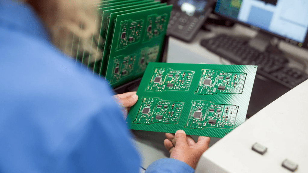
The significance of high quality PCB prototype cannot be overemphasized. This is very necessary if you desire high quality printed circuit boards.
In this article, we will be considering the applications of the high quality PCB prototype, benefits that manufacturers offer, as well as the steps involved in the whole process.
Applications of the High Quality PCB Prototype
Below are the applications of High Quality PCB Prototype
- High Quality PCB Prototype offers samples for your bulky productions for cases where there are defects in the design
- Manufacturing in small batches for research institutes and business makers. This will help in testing or selling the designs
- The Ceramic High Quality PCB Prototype is useful for applications requiring great thermal conductivity. These include automotive sensors, lasers, etc.
- Rigid-flex and Flexible High Quality PCB Prototype is useful for any device having compact space having the flexibility requirements, like satellites
- High Quality PCB Prototype of high frequency is useful for high speed/RF/ applications like antennas, and radars
- Aluminum High Quality PCB Prototype is useful for LED lights and power modules like the front lights of automotives
High Quality PCB Prototype Assembly and Manufacturing
High quality PCB prototype involve pre-production even before engaging in bulky or huge fabrication. Furthermore, the quality of this prototype has to be exactly the same as that of the bulky fabrication. At Rayming PCB & Assembly, when we get the gerber/IPC-2581 file from the customer, we have engineers that will review all the documents, if there is a need for improvement anywhere, then we will give suggestions and we will then hand you the quote. Once the customer reviews it and is fine with the process and agrees with the fabrication, then we can go ahead to manufacture your high quality PCB prototypes.
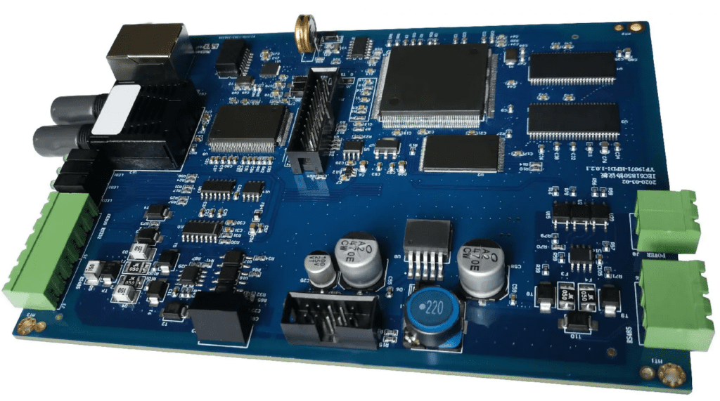
The process of high quality PCB prototype varies with respect to the different designs. However, they usually include pre treatment of the laminate, generation of the inner circuit, lamination, drilling, etching of the external circuit, printing of the solder mask, as well as surface finishing. Also, if you want us to offer high quality PCB prototype assembly, then we will make the SMT stencil as well as source the components of the electronic during the manufacturing of the PCB.
Furthermore, high quality PCB prototype assembly usually takes place on the company’s THT and SMT lines. In addition, the process of assembly includes printing of the solder paste, inspecting the solder paste, surface mount (high speed), surface mount (functional), reflow soldering, through hole mount, AOI inspection, wave soldering, aging test and functional inspection. If you desire, we also offer conformal coating.
Why should you choose a Reliable Manufacturer for your High Quality PCB Prototype?
Below are the benefits that high quality PCB prototype offer.
- High quality PCB prototype assembly and manufacturing happens on one factory line with mass and bulky production
- Strong capability for manufacturing. The company has two huge bases for PCB manufacturing as well as one
- The manufacturing process of high quality PCB prototype, delivery standards and testing are just like bulky production
- You will get one stop high quality PCB prototype, batch assembly and manufacturing, assembly of end product, and component sourcing
- One on one support for professional engineering all through the manufacturing, as well as assembly, of the customer’s project
- Complete and free PCBA sample for large and bulky orders, quick turn PCB prototyping
What are the Benefits of a high quality PCB prototype?
The whole area of the high quality PCB prototype is just 0.2 meters and the necessary components are in small quantities as well, therefore high quality PCB prototype becomes fast. Here are some benefits
PCB prototypes allows developers to be able to test all the designs within a short time period and at affordable prices
High quality PCB prototype usually permits more optimization in huge manufacturing and make product manufacturing better
Offers free one on one support for engineering matters, DFX, DFT, and DFM to ensure the design has no defects.
Steps in Manufacturing a high quality PCB prototype
What are the necessary steps in manufacturing a high quality PCB prototype?
Design
This is the first step. You can make use of the software for PCB design in creating the design of the PCB. However, make sure that you indicate the software you have used when you have sent the package of the design
Bill of Materials
Developing the bill of materials is very important during the schematic phase. Here, all the components and materials required for high quality PCB prototype production are listed.
Routing Design
This is a subsequent step involving the high quality PCB prototype routing design. You will be able to achieve this by using the traces to connect all the printed circuit board’s elements.
Photo film development
The professionals will make use of whatever design you have provided in developing the high quality PCB prototype photo film making use of the right plotter or printer. This prints all the layers of the PCB as well as the solder mask.
Aligning the layers of the high quality PCB prototype
When there are multiple layers, then there is a need to align all these layers in an accurate manner before you punch the registration holes. Accurate alignment prevents the non-revision of the inner layers.
Fusing of the layers
This has to do with the fusing of the prepreg. This has to do with two major phases – The bonding phase and the layer up phase.
Holes drilling
This has to do with the drilling of the holes in the PCB stack which comes very important during the integration of the components later on. However, make sure there is precision.
Copper plating
This makes use of a chemical bath in integrating the copper layer in the PCB panel surface. This copper helps in shielding the entire panel; these include the interior walls of the holes.
Imaging the outer later
This allows you to image the outer layer of the high quality PCB prototype. This follows a very similar process.
Final Etching
This involves the removal of additional copper via a specific chemical reaction
Application of the solder mask
This is depositing more gold or silver plating.
Conclusion
High quality PCB prototype is very important for all PCB projects. They are also relevant in different applications.
